Circuit Printing with Squink
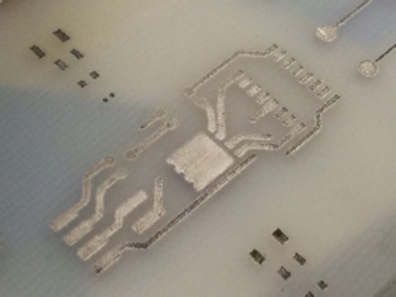
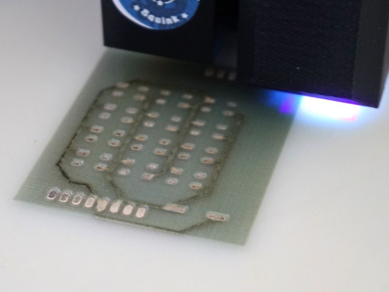
Squink inkjet prints low resistivity conductive inks and dielectric insulating inks so that you can prototype Printed Circuit Boards (PCBs) in minutes on a variety of stiff and flexible substrates. As a Circuit Printer, Squink sequentially prints conductive traces and then insulating layers, leaving gaps in the dielectric to act as vias and allow electricity to flow between layers.
Instead of waiting for weeks or shelling out thousands for factory-made PCBs, load Gerber or image files (JPEG, BMP, PNG) into the printer's web interface and have electronic circuit boards printed in a variety of substrates in minutes! Think of the possibilities with printing flexible lighting on clear films, creating flexible multilayered circuits, or teaching your students the fine art of PCB prototyping and design - all of this

Specifications
- Nanoparticle silver ink
- Cured by heat
- Create single-layer circuits (or multilayer with the Squink Multilayer PCB Printer)
- Print on FR-4 and Kapton, or any material treated with Insulating Ink and does not warp or melt at 150 Celsius or bellow.
- Sheet Resistance: 40
mOhms /square - Minimum Trace Pitch: 30 mils / 0.76 mm
- Minimum Trace Width: 10 mils / 0.25 mm
- Compatible with:
There may be specific applications for Squink in your research or work. If you have questions about printing on a specific material, printing with specific inks, printing finer traces than 10 mils, or printing more than 2 layers please reach out to us.
Conductivity
| Trace Width | Recommended Amperage (@ 5V) | Max Amperage (@ 5V) |
| 10 mil (0.25 mm) | 240 mA | 340 mA |
| 15 mil (0.38 mm) | 840 mA | 840 mA |
| 20 mil (0.5 mm) | 1.1 A | 1.6 A |
| 30 mil (0.75 mm) or greater | 1.7 A | 2.4 A |
Working Print Area
| Number of Layers | Working Area (Metric) | Working Area (Customary) |
| Single | 127 x 127 mm | 5" x 5" |
| 2 - Layers | 85 x 127 mm | 3.35" x 5" |
- Polymeric Ink
- Cured by UV light (provided by Multilayer head)
- Compatible with Advanced Ink for fabricating Multilayer PCBs
- Print on any flat, non-porous surface
- Compatible with:

"We are conducting research into combining electronics with additive manufacturing. The Squink’s ability to print circuit traces from PCB design software (we use Eagle and KiCad currently) is important to us. We are using it as a research tool to print traces onto a variety of substrates...[ ] ... The Squink is a very nice and well-engineered tool for the price point."
-Michael Whitley, VP of Engineering, EngeniusMicro
