Our core competency is in integrating maturing technologies to miniaturize PCB manufacturing so that it may fit on your desktop. We are using everything from additive manufacturing (or 3D Printing) to Nanotechnology to image-recognition algorithms, creating a solution that is larger than the sum of its parts: BotFactory Squink.

Nanoparticle Silver Ink
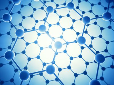
Since Richard Feynman stated 'There's Plenty of Room at the Bottom' in 1959, Nanotechnology has grown to outsized proportions. BotFactory has taken lessons learned in the lab and applied them to industrial problems, like PCB Prototyping and Production. Married with an Inkjet 'Direct-print' system, it is possible to print conductive traces at your desktop, straight from your PCB Gerber files. In addition to FR4 and Polyimide, it is possible to print on smooth, nonporous surfaces like Acrylic or PET.

Digital Stencil and Solder-Masking
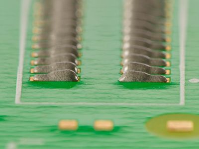
Masks should be a thing of the past - directly applying solder pastes and conductive glues where they are needed could be how PCBs are prototyped in the future. This is why BotFactory integrates a dispensing system into their trace-printing and pick-and-place functionality to provide an end-to-end solution for PCB prototyping and fabrication. After uploading a mask image or Gerber paste/solder file, you can cover your entire board in minutes, dispensing from a syringe with a fine tip in a carefully controlled manner.

Desktop PCB Assembly
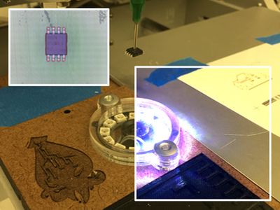
The key element of automated assembly of a PCBA is rapid yet repeatable identification of each Surface Mount component (SMD), using a camera and image-recognition software. We place the graphics-processing on board each machine, reducing any potential lag caused by an operator's computer. BotFactory expended a great amount of resources on creating scalable yet light-weight image-recognition algorithms capable of assembling the whole universe of SMD components, from 0603 to SOIC-24.
The Future of Electronics is here
Squink simplifies product development and saves you time and money
