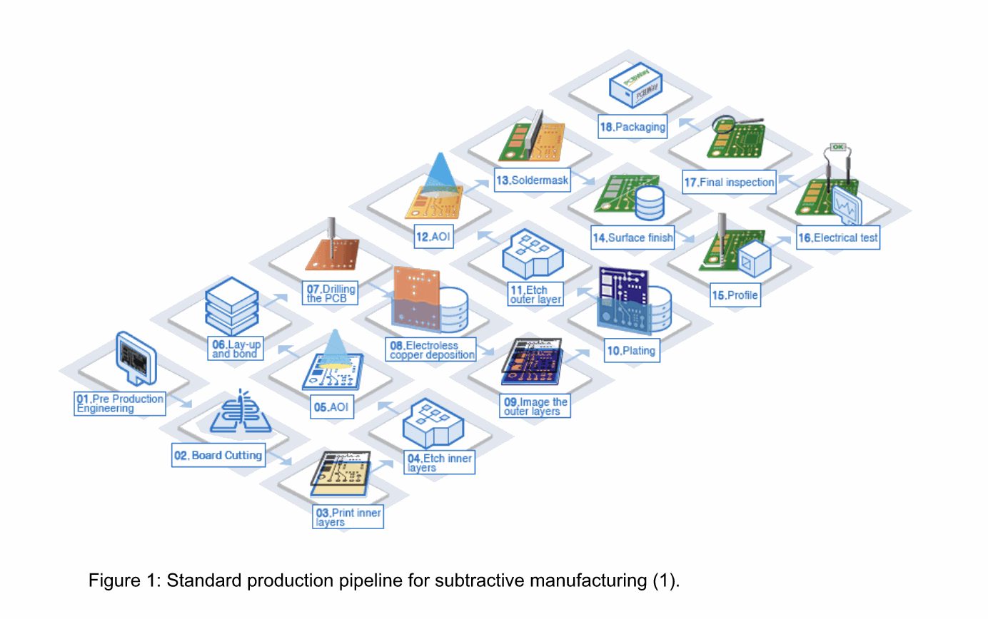
The whole process involves approximately 18 stations in the pipeline and is extremely rigid, time-consuming, and expensive. The process has been the standard to date and has been extremely reliable for manufacturing at scale. This immense market opportunity, over the past few decades, has intrigued researchers to perform cutting-edge research for developing complex PCBs and they have found methods to additively manufacture layers to create a whole different methodology for manufacturing PCBs, which has the potential to become the next stage of evolution from its predecessor, subtractive manufacturing (SM).
Problems with Subtractive Manufacturing (SM)
The subtractive process has multiple issues that were previously not possible to address due to lack of technology development. The primary issues are discussed below.
Lack of Design Flexibility
First and foremost, the SM method does not allow changing the volumetric density of the substrates. Secondly, there are restrictions on the number of features that can be used in the design and manufacturing processes, which means there is no support for odd geometries. This also means that rapid iterations to launch products faster are not possible.
Environmental hazards that arise from pre and post processing PCBs
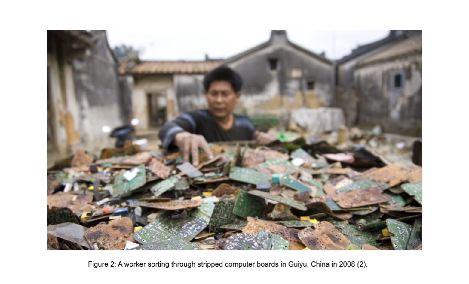
During the whole product lifeline of a PCB, extreme amounts of material wastage take place. This not only happens in the manufacturing pipeline, but also, when the PCBs are discarded or burnt, where a lot of materials and hazardous chemicals are used and are then wasted in addition to the PCBs themselves.
These pollutants have been contaminating clean water with heavy metals and organic matter, creating massive amounts of toxic waste worldwide.
Lack of Production Flexibility and High Costs
Researchers around the world have been exploring various avenues within the additive manufacturing field to develop time-saving, cost-effective solutions to produce PCBs that have more freedom in design choices within a compact printing setup, which extrudes layers of materials to form a PCB. The technologies used in additive manufacturing comprise integration between machine vision, artificial intelligence, and extremely precise robotic control units, which allow for extremely fine material flow with nanometer accuracy. This allows for the creation of layers of PCBs within a compact and complex form factor. The robustness of these printers has been gaining the trust of institutions that design high-end advanced PCBs with extremely complex features, which were not previously possible with the traditional manufacturing methods. The benefits of 3D-printed PCBs within the advanced layers of circuit board designs are discussed in the next section.
Benefits of using 3D-printed PCBs for advanced R&D
Design freedom
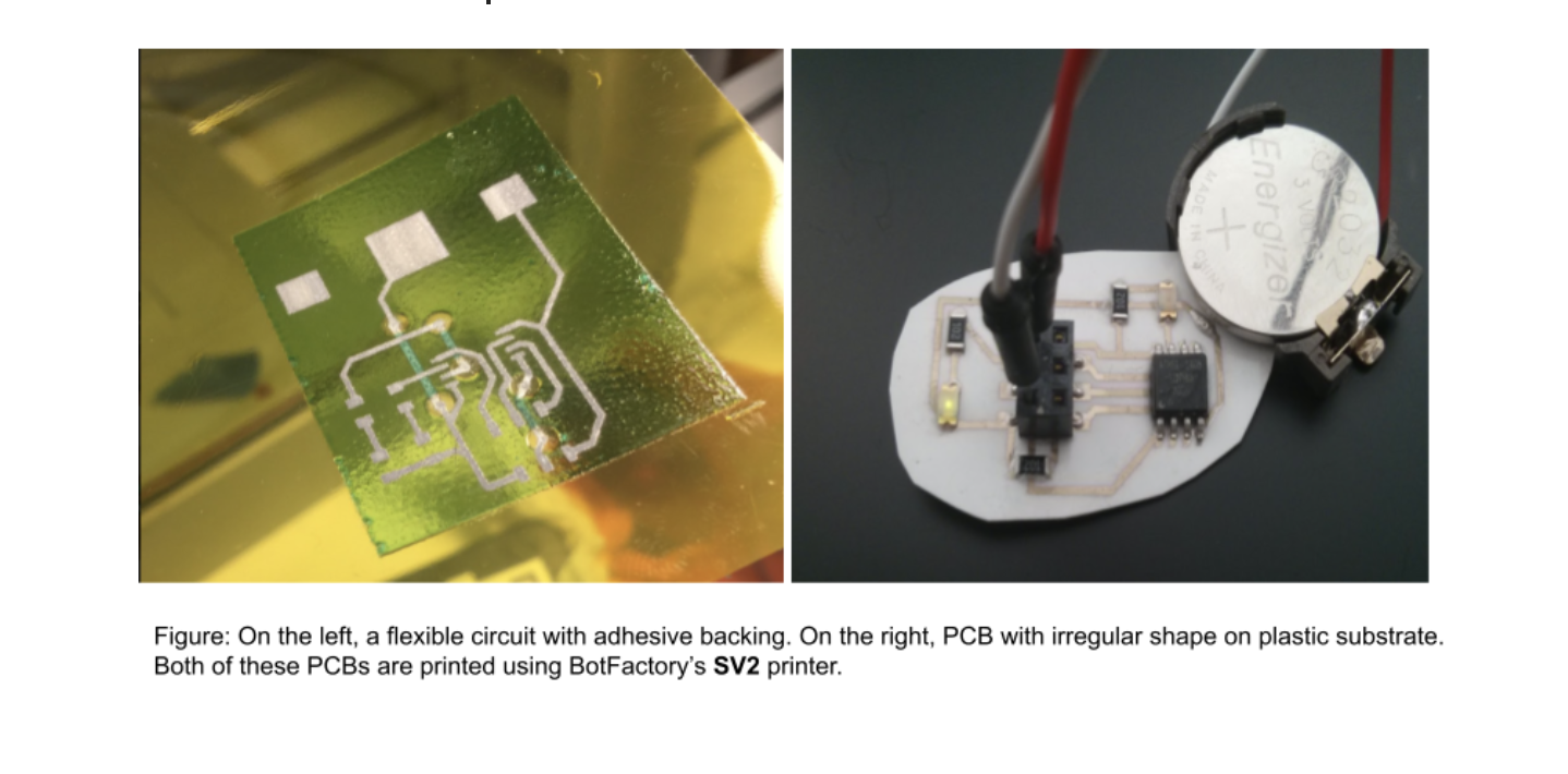
Because 3D-printed PCBs have no restrictions on the features an architect can include in their design, there is more freedom for experimenting with conductive and insulating layers than with traditional circuit boards.This means designers can create PCBs with various shapes and dimensions, with multitudes of complex layers in between.
Furthermore, design characteristics that add to the cost of the board in the traditional process (blind vias, higher layer count, buried vias, flexible substrates, rigid-flex substrates and milled features like slots and v-scores) are all minimal costs for the new fabrication technology, providing additional freedom to the designer.
Highly accurate, complex layers
The extremely accurate gait movements of the printing path means 3D printers can reliably print traces of around 8 mils (200 microns) with more compact trace gaps and vias within a smaller printable area. In addition, since there are no fundamental limitations to the number of layers a printer can print,the volume of interconnections can be further increased per square inch, at a reasonable cost, allowing for more compact form factors.
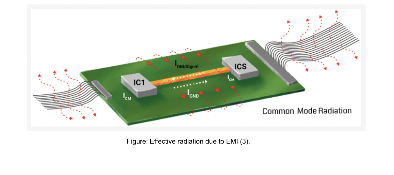
Resistance to EMI
Substrate selection/flexible substrates
Multi-material Print
3D printing enables use of various different types of inks and there is a possibility of having an endless choice of materials. Researchers have shown possibilities of printing with wide variety of inks with different applications, such as:
- Resistive inks to print and replace traditional resistors.
- Semiconductive inks to create high-performance transistors.
- Organic inks to print OLEDs.
- Inks made of Piezoelectric material, and so on.
The usage of such material combinations in summary, would slowly but certainly be able to replace components and reduce the complexity of the "bill of materials".
Production speed
With 3D printers, PCB production time is counted in hours rather than weeks since in-house production with flexible design choices can be performed. The choice of having an in-house printer allows for better collaboration between engineers, from circuitry design to mechatronics integration to prototyping and various iterations, significantly speeding up the entire pipeline and market rollout.
Keeping intellectual property safe
Since 3D printing can be done in-house, there is no need to outsource PCB production, allowing for greater product design confidentiality. Removing this issue from the project pipeline altogether means, the implementation of regulatory measurements (red tape) can be seriously reduced as well, decreasing the overall budget for task completions.
Environmentally friendly/waste reduction
The use of subtraction methods requires various grades of hazardous chemicals and produces a lot of waste. In addition, the restriction of design choices wastes board space and resources. Creating more compact 3D-printed PCBs means less material waste and a more efficient use of resources. In addition, researchers have been pushing the use of non-hazardous recycled materials for printing, which makes the whole process much safer and healthier.
It should be noted that traditional manufacturing is becoming increasingly expensive because countries are implementing regulations to reduce water wastage and are requiring water treatment after the process to reduce water pollution.
The ability of an organization to have a clean manufacturing process is an additional advantage that can hedge future regulatory requirements.
On-Demand Printing
The freedom to design and use a printer whenever required means a large inventory setup is not required for PCB manufacturing on a small scale. This not only creates a more agile product development process but also reduces commitments to third parties for large orders and eliminates the chance of supply chain disruption.
Challenges ahead for 3D-printed PCBs in Advanced R&D
Material Suitability
As the technology is still relatively new and many of the components are still not robust, a range of suitable materials are still being experimented with for developing reliable PCBs as mentioned in the benefits sections. Since this is still at an early stage, researchers have been conducting various tests on materials to prove concepts in a wide range of applications but finding many bottle-necks, such as:
- Even though AM has allowed for more materials to be worked with, joining and testing various materials for different applications are at early stages of development. This means the end users do not trust 3D printed PCBs as much as its counterpart.
- From a product development/project management aspect, adding 3D printed PCBs in the work packages involves more risks for the stakeholders. This takes a lot of ‘inertia’ to overcome and often triggers ‘change controls’ in ongoing projects. This puts a lot of strain on the economic limits of development.
Lower Conductivity
For 3D printing, silver-based conductive inks are more widely used, which are usually mixed with other mediums to create proprietary inks for various 3D printer manufacturers that allow for better absorption on substrates. The trade-off allows for lesser conductivity compared to traditional printing, which has more pure copper layers after being etched.
The lesser conductivity are affected by two sources:
- The added materials to make it into an "ink" reduces conductivity
- more importantly, the layers deposited are thinner 4um (our board) vs 35um (a typical board)
Restricted board size
3D printers can currently only produce PCBs that are as large as the printer chamber allows, which can limit some design factors. Thus, large circuit boards are sometimes challenging to accommodate for printing. That said, knowing the 2D plane boundary allows flexibility in designing with more layers, which the 3D printers are really good at doing.
BotFactory Efforts
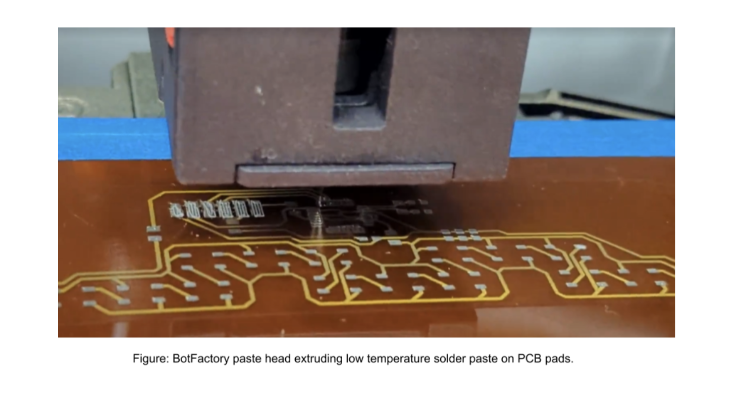
About BotFactory
BotFactory is the leader in desktop additive manufacturing of electronics, offering machines capable of printing multi-layer PCBs, dispensing paste, and picking and placing components in a single system. BotFactory's solutions enable on-site and same-day manufacturing for R&D teams worldwide.
References
1. “PCB Manufacturing Process and Equipment - PCBWay.” PCB Manufacturing Process & Equipment - PCBWay, www.pcbway.com/pcb-service.html. Accessed 22 Nov. 2022.
2. Hub, Asia P3. “Turning the Toxic Tide of Printed Circuit Board E-Waste.” Medium, 23 July 2019, medium.com/asia-p3-hub-updates/turning-the-toxic-tide-of-printed-circuit-board-e-waste-65634ed4256f.
3. Team, The Sierra. “Tips and PCB Design Guidelines for EMI and EMC | Sierra Circuits.” Sierra Circuits, 28 Aug. 2020, www.protoexpress.com/blog/7-pcb-design-tips-solve-emi-emc-issues.
4.Global printed circuit board market to hit sales of 91.87 billion by 2028: Faulty PCB to remain a key challenge: Skyquest Technology (2022) Barchart.com., https://www.barchart.com/story/news/10418649/global-printed-circuit-board-market-to-hit-sales-of-9187-billion-by-2028-faulty-pcb-to-remain-a-key-challenge-skyquest-technology (Accessed: November 30, 2022).