The printed circuit board (PCB) manufacturing industry generates substantial wastewater containing hazardous chemicals and materials, posing significant environmental challenges throughout its lifecycle. As global PCB production expands, the impact of this waste becomes more pronounced, necessitating effective wastewater treatment and sustainable manufacturing practices.
Additively manufactured PCBs, also known as 3D-printed PCBs, are revolutionizing the industry by reducing waste and enabling more efficient production processes. These advanced techniques minimize the use of harmful chemicals and materials, contributing to a more sustainable manufacturing approach. In this blog we will discuss the barriers to local PCB manufacturing, the complexities of PCB recycling, the waste generated throughout the PCB lifecycle, mitigation strategies for PCB waste, environmental impact assessments, and the revolutionary potential of 3D PCB printing.
Waste created from PCB lifecycle
The lifecycle of printed circuit boards (PCBs) generates various types of waste at different stages, from production to disposal. Here is an overview of the waste created throughout a PCB's lifecycle:
| Stage | Waste Generated |
| Manufacturing | Chemical waste (etching solutions, solvents), metal waste (copper, tin), plastic waste, wastewater |
| Use | Minimal waste during normal operation |
| End-of-Life | E-waste containing hazardous materials (lead, mercury, cadmium) |
| Recycling | Residual materials not recovered, chemical waste from recycling processes |
During the manufacturing stage, PCB production creates significant chemical waste from etching solutions and solvents used in the fabrication process. Metal waste, primarily copper from edge trims and spent etching solutions, is also generated. Wastewater containing various contaminants is a major byproduct, with approximately 1500 liters of water used to produce 100 iPhone-sized PCBs.
While PCBs generate minimal waste during their operational life, the end-of-life stage presents substantial environmental challenges. Discarded PCBs become part of the growing e-waste stream, containing hazardous materials such as lead, mercury, and cadmium. These substances can leach into the environment if not properly managed, potentially contaminating soil and water sources.
The recycling process, while aimed at recovering valuable materials, also generates waste. Not all materials in PCBs can be effectively recycled, leaving residual waste. Additionally, some recycling methods, particularly hydrometallurgical techniques, produce chemical waste that requires proper treatment and disposal.
PCBs' durability, designed to withstand harsh conditions during use, ironically contributes to their persistence as waste. The complex mixture of materials and the presence of hazardous substances make PCBs challenging to recycle completely, often resulting in a portion ending up in landfills or incinerators. (1) (2)
Environmental Impact Assessment
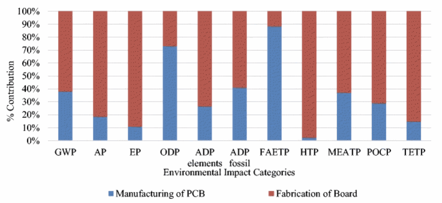
The environmental impact of printed circuit board (PCB) manufacturing is significant and multifaceted, as revealed by recent studies and industry data. A life cycle assessment (LCA) study conducted on a PCB manufacturing plant in Turkey provides valuable insights into the environmental burdens associated with this process.
The study identified two main stages in PCB production: board fabrication and PCB manufacturing. Board fabrication, which involves preparing the board with materials like copper, glass fiber, and epoxy resin, was found to be the primary contributor to several environmental impact categories. These include Human Toxicity Potential (HTP), Eutrophication Potential (EP), Terrestric Ecotoxicity Potential (TETP), Acidification Potential (AP), and Global Warming Potential (GWP). PCB manufacturing, encompassing processes such as circuit printing, etching, solder masking, and protective coating, significantly contributes to Freshwater Aquatic Ecotoxicity Potential (FAETP) and Ozone Layer Depletion Potential (ODP). Notably, etching operations were identified as a major hotspot, responsible for 89% of FAETP and 73% of ODP impacts, primarily due to the disposal of copper-containing wastewater treatment sludge and the use of hydrochloric acid (HCl).
Water consumption in PCB manufacturing is substantial. On average, 1.5 cubic meters of clean water are used per square meter of PCB produced. To put this into perspective, producing 100 PCBs the size of an iPhone 15 requires approximately 1500 liters of water, or 15 liters per iPhone-sized PCB. This high water usage contributes to the industry's significant environmental footprint.
The manufacturing process also involves extreme conditions that necessitate highly durable materials. PCBs must withstand heavy chemicals and acids, multiple cycles of high temperatures (180°C-400°C) during lamination, and high pressure cycles (0.3-1.0 MPa). Additionally, they must be fire retardant. These requirements result in PCBs that are extremely durable - "built better than a tank" - but also incredibly difficult to recycle. The study recommends focusing on in-plant control of etching operations and emphasizing copper recycling during the etching process to mitigate environmental impacts. These measures could significantly reduce the negative effects on FAETP, Abiotic Depletion Potential (ADP) fossil, and other environmental categories.
However, the durability of PCBs presents a significant challenge for end-of-life management. Their resistance to degradation means they often end up in inappropriate disposal sites after their useful life, potentially leading to long-term environmental contamination.
In conclusion, while PCBs are essential components in modern electronics, their production and disposal pose substantial environmental challenges. Addressing these issues requires a comprehensive approach, including improved manufacturing processes, advanced recycling technologies, and stricter regulations on disposal and handling of electronic waste containing PCBs. (3)
Current Mitigation Strategies
Current methods for mitigating PCB lifecycle waste issues focus on improving manufacturing processes, enhancing recycling techniques, and developing more sustainable design practices. Here's an overview of key mitigation strategies:
| Current Mitigation Strategy | Description |
| Wastewater Treatment | Advanced filtration systems like those offered by Hongtek Filtration Co., Ltd. remove contaminants, heavy metals, and organic matter from PCB manufacturing wastewater. |
| Green Manufacturing | Adoption of less toxic materials and processes, such as lead-free soldering and water-based cleaning agents, to reduce hazardous waste generation. |
| Design for Environment (DfE) | Incorporating eco-friendly design principles to make PCBs easier to recycle and less harmful at end-of-life. |
| E-waste Recycling Programs | Establishment of formal e-waste collection and recycling programs to prevent improper disposal of PCBs in landfills |
| Advanced Recycling Technologies | Development of methods to recover both metallic and non-metallic components from PCBs, such as pyrolysis and hydrometallurgical processes. |
| Extended Producer Responsibility (EPR) | Policies requiring manufacturers to take responsibility for the entire lifecycle of their products, including disposal and recycling. |
| Regulatory Compliance | Stricter enforcement of regulations like RoHS (Restriction of Hazardous Substances) to limit the use of harmful materials in PCB production. |
| Waste Reduction Initiatives | Implementation of lean manufacturing principles to minimize waste generation during PCB production. |
These mitigation strategies aim to address the environmental challenges posed by PCB waste throughout its lifecycle. For instance, advanced wastewater treatment systems can significantly reduce the release of toxic substances into water bodies. Green manufacturing practices help minimize the use of hazardous materials from the outset, while improved recycling technologies enable better recovery of valuable materials from end-of-life PCBs.
Design for Environment principles are particularly promising, as they consider the entire lifecycle of a PCB during the design phase. This approach can lead to PCBs that are easier to disassemble and recycle, potentially reducing the amount of waste that ends up in landfills.
Extended Producer Responsibility policies are gaining traction globally, encouraging manufacturers to consider the environmental impact of their products beyond the point of sale. These policies can drive innovation in product design and recycling technologies.
Despite these efforts, challenges remain. The complex composition of PCBs and the rapid pace of technological change continue to pose difficulties for recycling and waste management. Ongoing research and development in areas such as bio-based PCB materials and more efficient recycling processes are crucial for further mitigating the environmental impact of PCB waste.
Ultimately, a combination of technological innovation, regulatory measures, and industry-wide commitment to sustainability is necessary to address the waste issues associated with PCB lifecycles effectively. (4) (5) (6)
3D PCB Printing Revolution
3D PCB printers are revolutionizing the landscape of waste management in the electronics industry by offering a more sustainable and efficient approach to PCB production. This innovative technology addresses several key environmental concerns associated with traditional PCB manufacturing methods.
Firstly, 3D PCB printing significantly reduces material waste. Unlike subtractive manufacturing processes that remove excess material, additive manufacturing used in 3D PCB printing only deposits the necessary materials, minimizing waste generation. This approach aligns with the principles of the circular economy, promoting resource efficiency and reducing the environmental footprint of PCB production.
The technology also minimizes the use of harmful chemicals and reduces water consumption. Traditional PCB manufacturing involves extensive use of etching chemicals and large volumes of water for cleaning and processing. In contrast, 3D PCB printing employs specialized conductive and dielectric inks, eliminating the need for etching chemicals and significantly reducing water usage.
| Environmental Aspect | Traditional PCB Manufacturing |
3D PCB Printing |
|
Material Waste |
High (subtractive process) |
Low (additive process) |
|
Chemical Usage |
Extensive etching chemicals |
Minimal (specialized inks) |
|
Water Consumption |
High (1.5 m³ per m² of PCB) |
Significantly reduced |
|
Energy Efficiency |
Lower |
Higher (on-demand production) |
3D PCB printing enables on-demand production, reducing overproduction and associated waste. This capability is particularly beneficial for prototyping and small-scale production, allowing designers to iterate quickly without generating excess waste from multiple production runs.
Moreover, the technology opens up new possibilities for PCB design that can enhance recyclability. By enabling the creation of more complex structures and the integration of multiple materials, 3D PCB printing could potentially lead to designs that are easier to disassemble and recycle at the end of their lifecycle.
The adoption of 3D PCB printing also addresses some of the barriers to local manufacturing. By reducing the need for extensive chemical processes and large water treatment systems, it makes small-scale, local PCB production more feasible. This localization can lead to reduced transportation emissions and a more distributed, resilient supply chain.
While 3D PCB printing technology is still evolving, its potential to transform waste management in the electronics industry is significant. As the technology matures and becomes more widely adopted, it could play a crucial role in mitigating the environmental impacts of PCB production, aligning the industry more closely with circular economy principles and sustainable manufacturing practices. (6) (7)