The electronics industry is on the cusp of a new era, marked by the rise of organic and printed electronics. These innovative technologies are set to redefine what's possible in electronic design and application, offering a stark contrast to traditional, rigid electronics.
Understanding Organic and Printed Electronics
Organic electronics, composed of carbon-based compounds, boast inherent flexibility that traditional metal and glass substrates cannot match. This flexibility paves the way for groundbreaking applications in wearable technology, flexible displays, and medical devices that can mold to the human body's contours.
Printed electronics take this a step further by printing electronic circuits onto various substrates using conductive inks. This scalable method mirrors the roll-to-roll printing process of newspapers, leading to electronics that are not only lightweight and flexible but also potentially disposable.
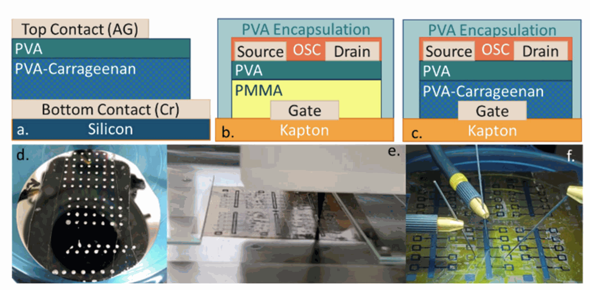
Figure 1: This image illustrates the innovative approach to organic electronics with a focus on green materials. It shows (a) the cross-section of a Metal-Insulator-Metal (MIM) test capacitor, (b) and (c) the cross-sections of Organic Thin-Film Transistor (OTFT) devices, and (d)-(f) photos of direct printed capacitor arrays and OTFT device arrays. The use of a low-temperature cross-linked polyvinyl alcohol (PVA)-carrageenan (CAR) layer as a green electronic gate dielectric is highlighted, demonstrating the potential for sustainable and flexible electronics (1).
The Traditional Divide
Traditional electronics manufacturing, with its reliance on rigid, inorganic materials, is a complex, multi-step process that includes etching, doping, and layering. These methods are not only costly and time-consuming but also limit the final product's form factors.In contrast, organic and printed electronics utilize simpler, additive processes that deposit material only where needed. This method is more sustainable and cost-effective, especially for designs where flexibility and form factor are crucial.
Industry Research and Technology Readiness Levels (TRLs)
The industry's exploration of organic and printed electronics spans various Technology Readiness Levels (TRLs), from basic research to proven systems in operational environments.

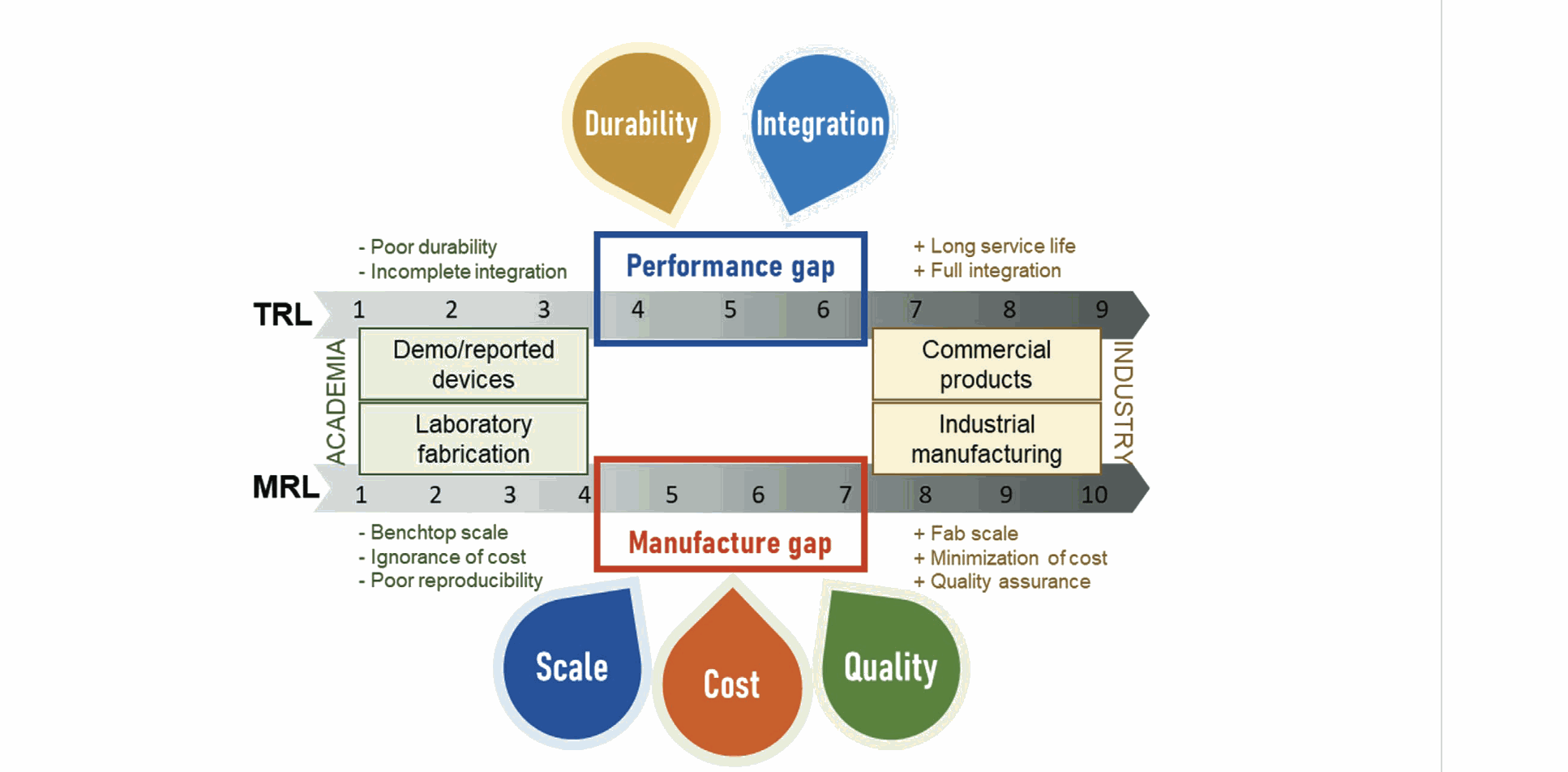
Figure 2: Gaps in device performance and manufacture capability between flexible electronics in academia and industry, as assessed by TRL and MRL. This image from "Devising Materials Manufacturing Toward Lab-to-Fab Translation of Flexible Electronics" illustrates the challenges in bridging the gap from lab to fab, highlighting areas such as durability, integration, scale, cost, and quality that need to be addressed (3).
At lower TRLs, the focus is on new materials and printing techniques to improve organic and printed electronics' performance and reliability. As TRLs progress, the emphasis shifts to integrating these technologies into functional prototypes and pilot projects, testing their real-world applications and durability.
BotFactory's SV2 Printer plays a crucial role in this innovation spectrum, providing a vital tool for testing, prototyping, and iterating organic and printed electronic devices. The SV2 Printer enables rapid creation and modification of prototypes, thus accelerating the development cycle and bridging the gap between low and high TRLs.
For example, the SV2 Printer was instrumental in the development of laser-induced graphene pressure sensors, which are highly sensitive and cost-effective for health and environmental monitoring applications (2).
Bridging the Gap: BotFactory's Role in the Performance and Manufacturing Divide
BotFactory is acutely aware of the performance and manufacturing gap highlighted in Figure 2. We are actively listening to the needs of printed and organic electronics manufacturers and are committed to creating and optimizing our tools for inspection, prototyping, and iteration to support the industry's transition to commercial and industrial products and manufacturing processes.
BotFactory's SV2 Printer plays a crucial role in this innovation spectrum, providing a vital tool for testing, prototyping, and iterating organic and printed electronic devices. The SV2 Printer enables rapid creation and modification of prototypes, thus accelerating the development cycle and bridging the gap between low and high TRLs. For example, the SV2 Printer was instrumental in the development of laser-induced graphene pressure sensors, which are highly sensitive and cost-effective for health and environmental monitoring applications (2). Read more here

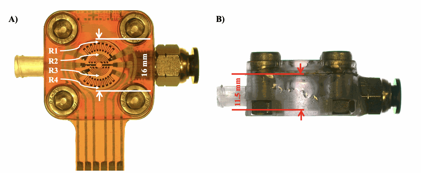
Figure 3: Close-up top view of a fully assembled circular diaphragm pressure sensor with resistor locations (A) and side view of the assembled sensor showing the stack order: Test chamber bottom, gasket, sensor, then test chamber top (B). This figure demonstrates the BotFactory SV2's capability in producing intricate sensor components, contributing to the advancement of flexible electronics from prototyping to industrial application (2).
Conclusion
Organic and printed electronics are revolutionizing the electronics industry, opening up new avenues for innovation and design. As the industry delves deeper into the potential of these technologies, BotFactory's SV2 Printer emerges as an essential resource, facilitating the rapid iteration and refinement of 3d printed electronic circuit prototypes and sensors. With BotFactory's support, the path from concept to market-ready product is becoming more streamlined and efficient, heralding the arrival of the next generation of electronic devices.
References
- Massey, R. S., Song, X., & Prakash, R. (2023). Direct Printed Flexible Organic Thin-Film Transistors With Cross-Linked PVA-Carrageenan Gate Dielectric. IEEE Sensors Letters, 7(5), 4500804. https://doi.org/10.1109/LSENS.2023.3271061
- Ivy, L., Gund, V., Davaji, B., Ospina, C., Ni, D., Doerschuk, P., & Lal, A. (2023). Laser-Induced Graphene Pressure Sensors Manufactured via Inkjet PCB Printer: Locally Producing Super-Sensitive and Cost-Effective Circular Diaphragm Pressure Gauges.
- Luo, Y., Wang, M., Wan, C., Cai, P., Loh, X. J., & Chen, X. (2020). Devising Materials Manufacturing Toward Lab-to-Fab Translation of Flexible Electronics. Advanced Materials, 32(34), 2001903. https://doi.org/10.1002/adma.202001903

