Making a 4-Layer Larson Scanner

– with the ATMEGA328P-AU

BotFactory Inc., Afnan Islam

Introduction

The classic Larson scanner effect—an LED array sweeping back and forth—has long been a favourite among electronics enthusiasts. Our previous project showcased how to print and assemble a simple two-layer Larson scanner PCB with the BotFactory SV2. Now, we’re taking it up a notch. The new design moves from a two-layer board to a four-layer stack swaps out the microcontroller for an Atmega328P-AU, and implements a host of improvements that push the boundaries of what you can achieve in-house.

Why Upgrade?

Our original design worked perfectly for a straightforward LED sequence. But as soon as we started imagining more features—additional sensors, more robust firmware, tighter routing, and improved signal integrity—we knew we needed more layers and a more capable microcontroller. The Atmega328P-AU, with its greater I/O and memory capabilities, gives us room to expand our code and add complexity. The four-layer PCB stack provides dedicated planes for ground and power, reducing noise and interference while making routing more efficient and flexible.

Refined PCB Layout

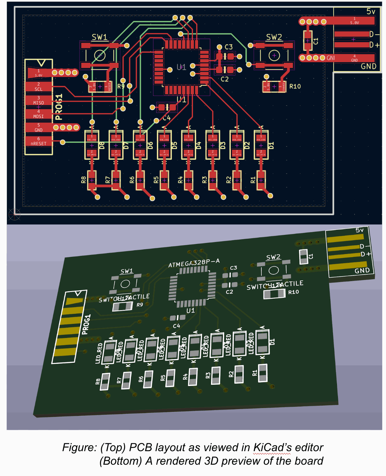
In moving to a four-layer configuration, we took advantage of cleaner signal paths, better EMI control, and the ability to separate sensitive analog signals from noisy digital lines. Power distribution is more stable, and ground currents no longer compete with signal traces, thanks to dedicated copper layers. These improvements translate into more reliable performance and open the door to integrating advanced features without worrying about signal integrity issues.

At the heart of it all is the Atmega328P-AU. This popular TQFP variant of the Atmega family is well-supported by toolchains like Arduino, making programming, prototyping, and iterating a breeze. We can easily refine LED patterns, incorporate sensors, and even add communication modules—all without redrawing the board from scratch.

Seamless Printing with the SV2

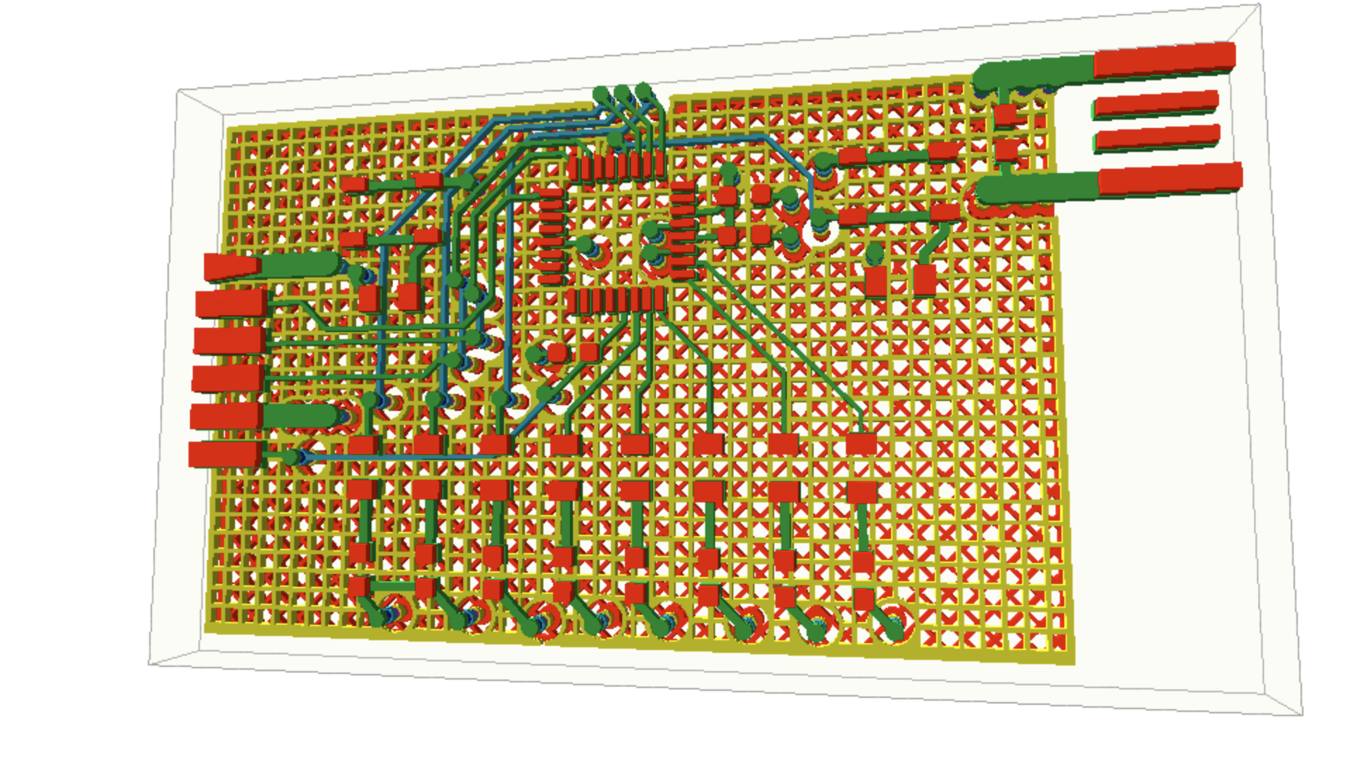
Even with the added complexity, fabrication on the SV2 remains straightforward. Export Gerber RS-274X files from KiCad, let the SV2 software run design checks, verify print height and curing settings, and hit print. Conductive inks and insulating layers build up each layer additively, so production times stay impressively short even with four layers. The design on the left highlights the ground planes, implemented in a mesh configuration—an easy edit in KiCad.

Post-Processing and Assembly

Once the four-layer board is printed, a quick manual cut brings it to final shape. Applying solder paste is still a snap: just swap to the solder paste dispensing head, align the nozzle, and let the machine do its work. The pick-and-place process hasn’t changed either, aside from handling a more complex component layout. The SV2’s camera-guided calibration ensures accurate placement of the Atmega328P-AU and any other fine-pitch components, as well as your LED arrays and support circuitry.

When it’s time to reflow, the heated bed ensures an even, consistent solder melt, leading to robust joints on every component. Even though the design has grown more advanced, the automation and flexibility of the SV2 let you handle it all in-house, on-demand, and without the long lead times or minimum order quantities you’d face with a third-party manufacturer.

Programming and Testing

After assembly, programming the Atmega328P-AU is as simple as connecting your programmer and uploading code using the Arduino IDE. The expanded memory and I/O let you try more complex LED patterns, implement smarter scanning sequences, or integrate sensors that react to their environment. The pins on the left of board have connections to the chip to connect an edge connector for programming. This helps with easy programming and reprogramming the chip when needed. 

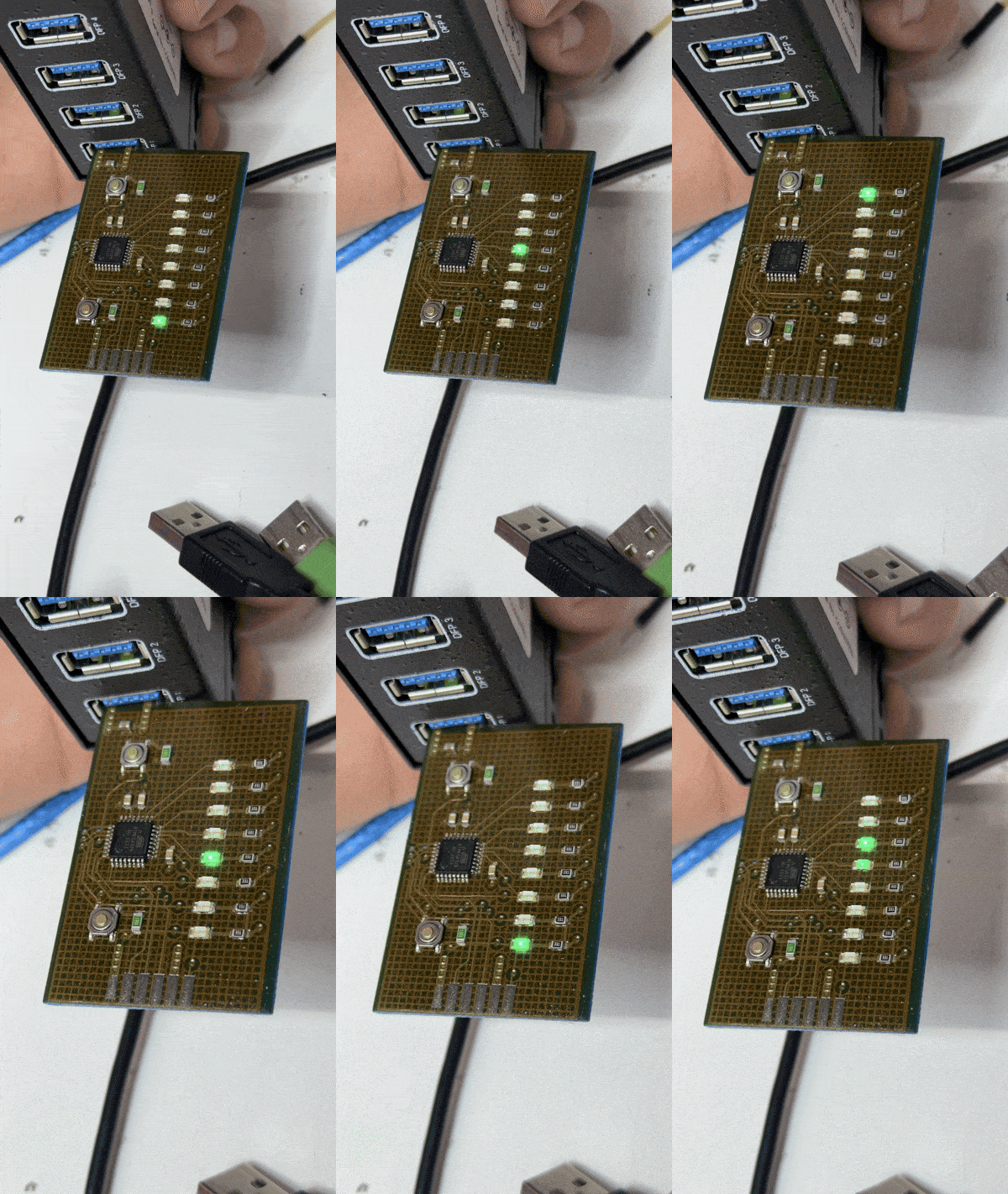
The result: a more dynamic, visually appealing Larson scanner effect—one that can be easily tweaked, upgraded, and expanded upon as inspiration strikes.

Taking Your Prototyping Further

This new four-layer Larson scanner is more than just a neat effect. It’s a demonstration of how quickly and effectively you can evolve your designs with the SV2. Need more power, more complexity, better EMI performance, or a richer feature set? Just redesign, reprint, and reassemble—no waiting, no outsourcing, and no compromises.

The upgraded design isn’t just about adding more layers or a better chip. It’s about unlocking the freedom to explore, refine, and push boundaries in your electronics projects—right at your own desk.