Cost Driver #1: Labor
Manufacturing PCBs is a complex process that requires highly-educated personnel at each step of the process. Engineers start the process by designing and submitting their files to a PCB manufacturer. Another engineer working at the PCB vendor will review the design submitted for fabrication, ensuring that there are no faults with the files and will consult with the customer to discuss any flaws found and to suggest design changes for their PCBs. The overhead cost of having highly trained engineers and technicians is reflected on the pricing given to the customer. Labor costs are relatively high for trained personnel in the US, which is why most manufacturing is done abroad where labor costs are lower.
PCB manufacturers have a team of engineers responsible for ensuring the submitted designs are without flaw, are suitable for the needs of the customer, and that the required tolerances of the fabricated boards are in-line with the industry standards set by bodies such IPC. Highly-trained technicians are also employed by manufacturers, they are responsible for running the equipment responsible for assembling the PCB. Technicians must continuously check the PCB while it is being fabricated in order to prevent any flaws that might slip through their strict controls.
Cost Driver #2: Distance
Manufacturing a PCB is a complex undertaking, especially when most PCB manufacturers are in another timezone, or even in a different continent. Due to the harsh chemicals used by PCB vendors, manufacturing PCBs seldomly happens within residential areas. If PCBs are produced in the USA or Europe there is an additional cost associated with complying to environmental laws as well as sourcing expensive base materials. Companies face costly fines if they are found at-fault for failing to comply with local ordinances and federal regulations. PCB manufacturers abroad face less rigid regulation and are able to source base material for a fraction of what domestic manufacturers pay.
Large and efficient supply chains between electronic component manufacturers, base material suppliers, and PCB manufacturers abroad allow for fierce competition and lower costs. If problems do arise, PCB manufacturers abroad can order replacement electronics or base materials locally and cut down setbacks by hours instead of days. However the main problem with ordering PCBs from foriegn companies is the time it takes to ship PCBs across the world. Shipping, customs, and taxes all cause delays in getting the finished products to the customer. Manufacturer’s offer expedited services for a high premium, most offer 24 hour services but the cost of having a shorter turnaround time significantly increases the total cost of the PCB and there are restrictions as to the complexity of the board.
.
Cost Driver #3: Complexity
The design of the PCB being manufactured introduces another difficulty in terms of lead times. Due to the complex processes required to achieve high quality PCBs, the more complex a board is, the more time that is required to make it. From one generation of electronics to another, Electrical Engineers are making devices smaller, more powerful and feature-rich, but unfortunately this increases the complexity of the board and thus introduces a higher risk for error. Features that increase the lead time of boards are the number of layers, hole sizes and hole-count, plugged/filled/micro vias, line geometry, controlled impedances, thickness of copper, and tight tolerances. These features can push the lead-time of a PCB from 1-2 days to 6 days or more, while also increasing the cost.
PCB Fabrication and Assembly Flowchart
The chart below shows the process used by most PCB manufacturers, information was gathered from various manufacturers and the processes that overlapped are shown. As you can see, the process of making a PCB is a long, complex process. Any flaw in the process means that the PCB fabrication must be restarted or hot fixes must be applied, this cost is absorbed by the manufacturer, so strict controls are placed between processes to prevent failures. Each process requires a highly trained specialist to ensure that there are no mistakes, this expense is reflected on the pricing the customer sees. This price also increases if the number of steps increase, which is the case for multi-layer boards and complex designs.
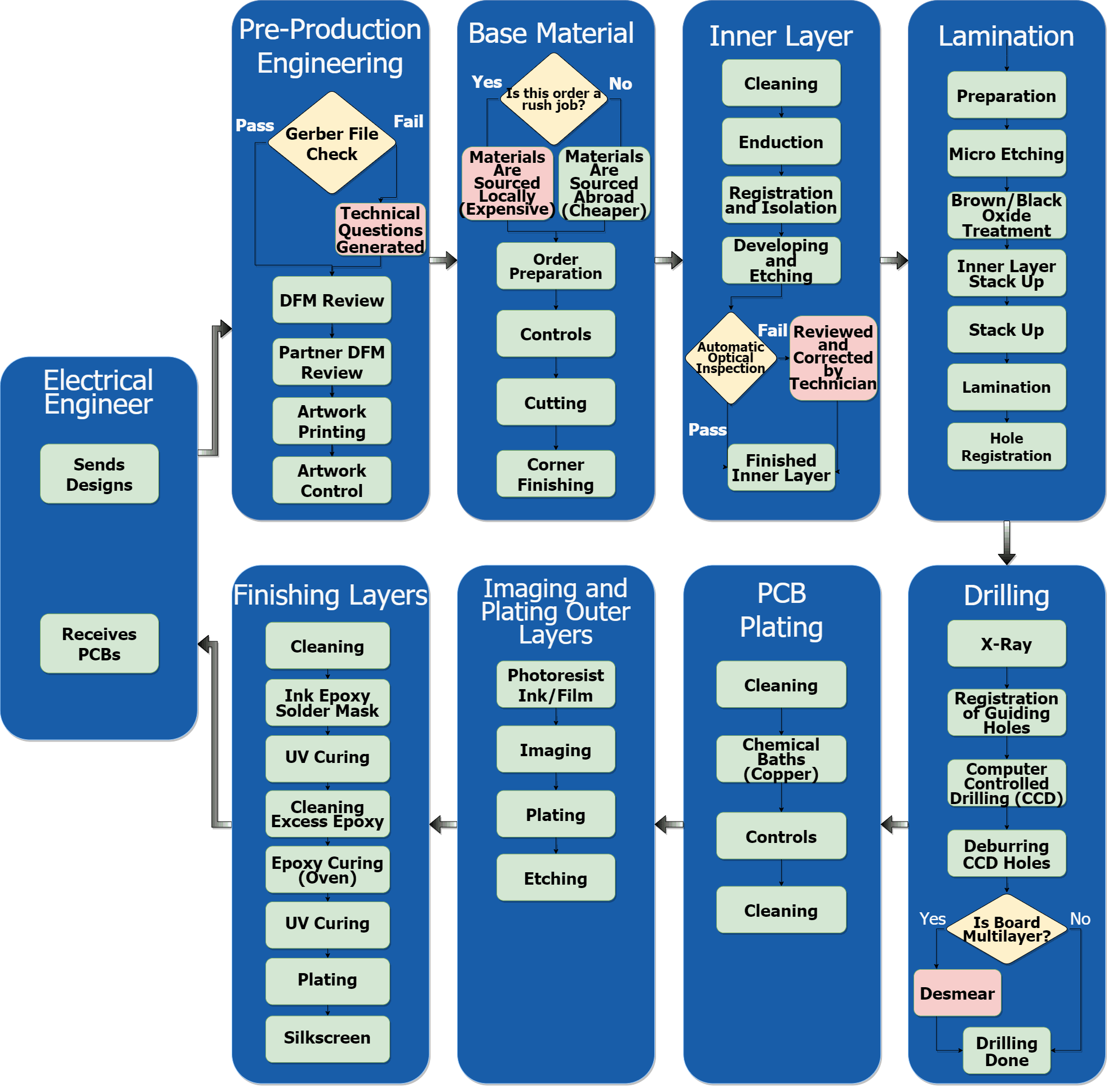
Increasing the number of layers raises the chance of internal layers shifting and ruining the fabricated board. Baking is a necessary step required to properly set multiple layers together, but this can cause the previous layer to shift and become misaligned or they can even cause the inner layers to shrink and change size. If a PCB board is complex and requires multiple layers the cost increases due to the usage of more material, more drilling, and repeating the plating processes required to form the individual layers. Having multiple layers is just one factor that can increase the complexity of a PCB, but unfortunately as you increase the complexity of a board the chance of a board developing an issue increases exponentially. As the complexity of boards increases, time required to manufacture the PCB rises due to added steps in the manufacturing process, this can result in lead times going from 1 day to 6 days, not including the time required for shipping the PCBs to the customer.
Printing and Assembly with BotFactory!
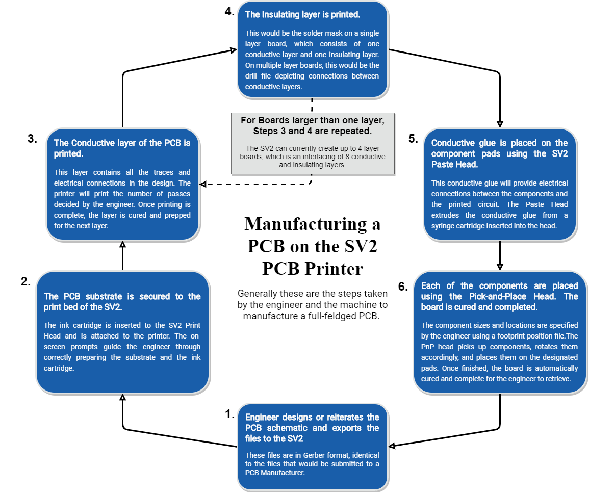
The flow chart above shows the PCB manufacturing process with the BotFactory SV2. The manufacturing process, when compared to the traditional manufacturing process, is streamlined to ensure the user can manufacture a board in a timely and cost efficient way. The traditional costs associated with labor and shipping PCBs from across the world are nearly erased with the SV2. Due to the simple and straightforward user interface, almost anybody can be trained to use the SV2 to fabricate a PCB in a short amount of time. The SV2 also allows electrical engineers to rapidly iterate on designs that would be too costly to justify allowing for engineers to innovate freely without bureaucracy.
The manufacturing process can be broken down into four main processes: conductive layer printing, insulating layer printing, solder paste dispensing, and pick-and-placing components. This streamlined method allows for turnaround times of a few hours, depending on the design of your board. This ability to redesign circuits and prototype them so quickly keeps engineers and companies agile and flexible to new constraints and design needs.