Additive 3D printing has revolutionized how we create physical objects, and PCB prototyping is no exception. From the start of Botfactory, our team has continuously focused on developing new features, methods, and test standards to provide our clients with the ultimate tool for PCB prototyping and manufacturing. Now you can quickly and seamlessly produce high-quality, double-sided substrateless PCBs that are cost-effective and easy to make using the SV2. In this blog post, we will discuss how we printed a 2 layered, double sided substrateless, Arduino Nano from scratch using the SV2 from BotFactory.
What is SV2?
For people who have not heard of the SV2, it is a 3D printer that has been specifically designed for creating PCBs. It uses conductive and insulating ink to print layers on any substrates of your choice. The printer is capable of printing double-sided, multi-layers, PCBs in various methods, allowing you to create complex circuits with ease. Today, we are focusing on how to use the SV2 for printing double sided boards on Kapton and peel the 3D printed board off to get you your first double sided PCB with multiple layers.

Creating Double-Sided Substrateless PCBs with SV2
Design your PCB
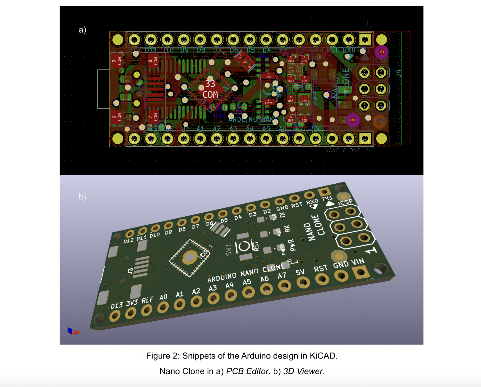
The first step is to design your PCB using a software tool. You can use a free tool like Eagle or KiCad to create your PCB design. Once you have designed your PCB, you can export it as a Gerber file. We designed an Arduino Nano clone and you can get the reference design from Arduino’s website. At Botfactory, we regularly use KiCAD for all our designs, which is an amazing toolkit for PCB designing PCBs for free. Some snippets are shown in Figure 2.
Configuration in the SV2 User Interface
Once you have your Gerber file, you need to load it into SV2's software interface which will verify your print (Figure 3), and run its own DRC (Design Rule Check). You must double check and readjust your design if needed if the DRC points out any substantial issues.

After verification, we always suggest you double check with the calibration if you haven’t used the printer recently or you are just getting started with the printer, the user interface will guide you through the process.
Now, the extremely important part. The trick to the whole double sided substrateless process is within the print configuration section as shown in Figure 3, and we suggest you print it on Kapton, the physics behind the surface tension between the materials is a whole different matter for another day. That said, choose the configuration to have the layers thick enough, so that the board is atleast 500 microns thick, which will be easily peelable from the Kapton, with no residue of the conductive traces from the bottom side left on the Kapton. For this specific board we printed with the following configuration for each layer:
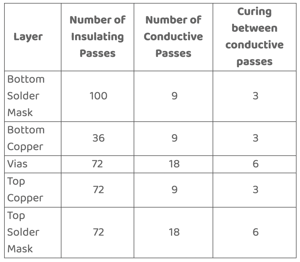
While printing, please remember you will have to cure between the passes with ideally a low temperature curing profile (Our R&D team have some new curing features coming out, so keep an eye). Otherwise, you might see weird artifacts building up on the printed structures. A snippet of the configuration within the software is shown in Figure 4.

You would also need to have both the top and bottom solder masks fwith enough conductive inks for the pads for a smooth peel off and soldering capabilities.
Printing Layers
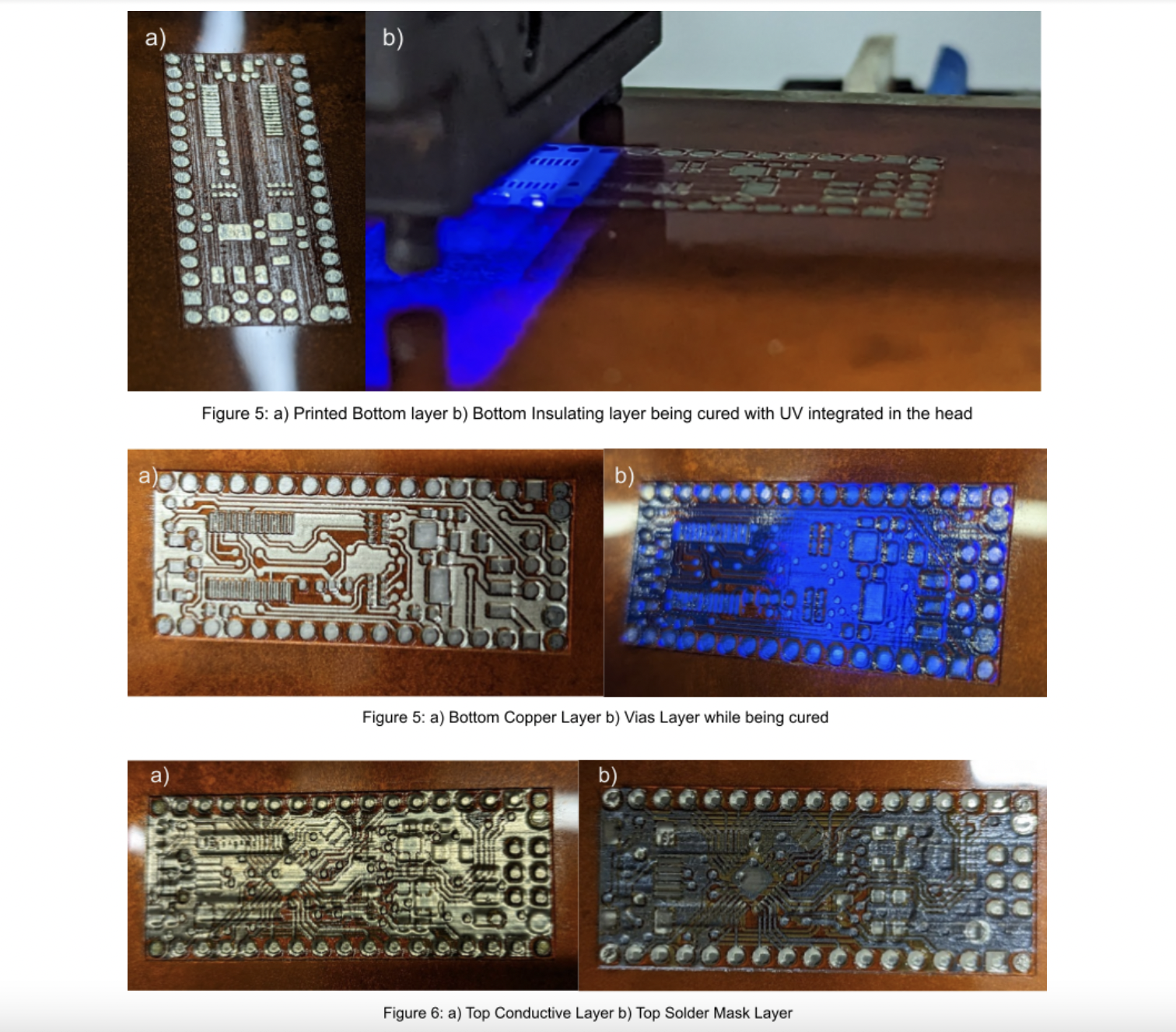
After configuration, you can start printing using the software interface. Please follow instructions to clean the inkjet cartridges and calibrate height with the header, since it is an intricate design which might fail midway. Please keep in mind you need to cure the ink between passes to make it stable and durable. The SV2 printer helps with the curing process by its built-in heatbed, which provides controlled heat to the PCB, helping the ink to bond to the layers and create a reliable PCB.
In Figure 4, 5 and 6, you can see all the results of the prints while the board was being developed. Images are zoomed in for better visualization.
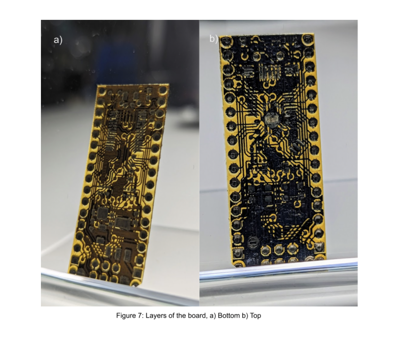
After the print is completed, and the board is cured, you can take the board off from the heatbed and slowly peel off the kapton from the board and not the other way around. You can reuse the Kapton again for multiple different prints. Finally, you will need to test the PCB to make sure that it is functioning properly. You can use a multimeter to check the continuity of the traces and make sure that there are no shorts or other issues.
You should have your freshly baked board ready for use as shown in Figure 6
Conclusion
3D printing double-sided substrateless PCBs using SV2 from BotFactory is an excellent way to create high-quality, cost-effective PCBs. The printer is easy to use and produces reliable, functional PCBs that are perfect for prototyping and small production runs. With SV2, you can quickly iterate on your designs and produce custom PCBs with ease.
For more information, please drop some details here, we will be happy to get back to you at our earliest convenience.