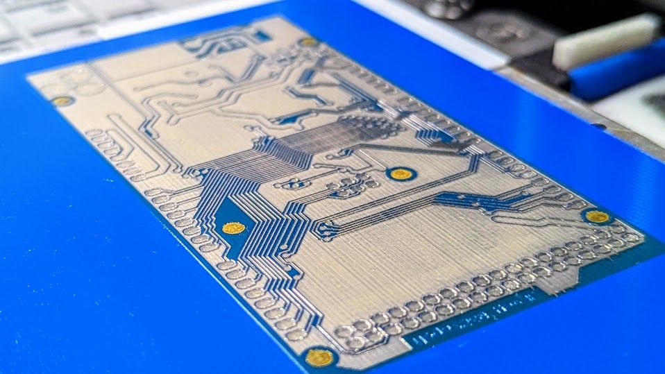
The Arduino Mega is a powerful microcontroller board renowned for its extensive capabilities, such as extra I/O pins, memory, and processing power, making it ideal for numerous complex projects. As BotFactory broadens its scope from prototyping to production, we're thrilled to highlight the SV2 Printer's ability to create custom single-sided Arduino Mega PCBs on FR4. This method offers a streamlined, efficient, and cost-effective solution for prototyping and small production runs.
A bit about the SV2..
If you're new to the SV2, welcome to this exceptional 3D printer for PCBs. The SV2 uses conductive and insulating inks to print layers on various substrates, allowing you to tailor your project materials. Capable of printing double-sided and multi-layered PCBs, the SV2 empowers you to craft intricate circuits with ease.
This article delves into the process of using the SV2 to print single-sided Arduino Mega circuits on FR4, a popular and versatile substrate for PCB applications. Through this comprehensive guide, you'll learn to create high-quality Arduino Mega PCBs on FR4 by leveraging the SV2's advanced features. Unlock new 3D printed PCB prototyping and production possibilities to elevate your project's efficiency and effectiveness.
Designing the Mega
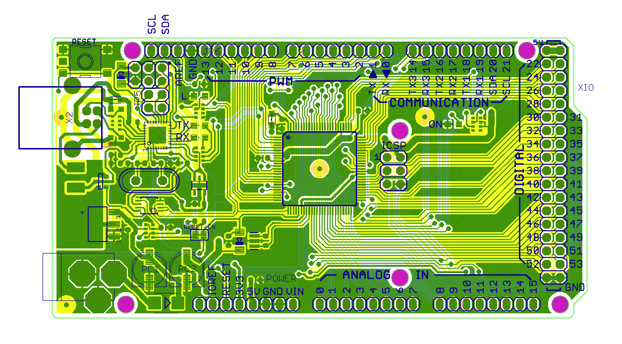
To begin designing the Arduino Mega PCB, we used KiCad, a powerful tool that offers extensive features and support for intricate designs. Although you can use any PCB design software, ensure it can generate Gerber files. Given the Arduino Mega's larger dimensions, increased pin count, and overall complexity, meticulous attention to detail is essential during the design process. On the right, you can see a complex design output from a PCB editor.
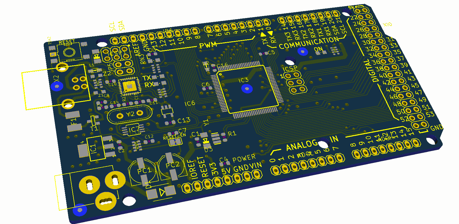
KiCad's 3D view option allows you to visualize your PCB design in great detail, as shown on the right. This feature is particularly helpful when preparing the design for printing with a high-precision printer like the SV2. The intricate details in the 3D file emphasize the level of accuracy needed for printing complex designs, such as the Arduino Mega.
When using the SV2 printer for your PCB prototyping needs, these details become even more critical. The printer's advanced capabilities, user-friendly operation, and rapid design iteration enable you to accurately reproduce the elaborate design from the 3D file. This ensures a high-quality, intricate PCB that meets the demands of today's cutting-edge projects. By carefully considering the design details in your design software and using the SV2 printer, you can successfully bring any project to life.
Configuring the SV2 User Interface
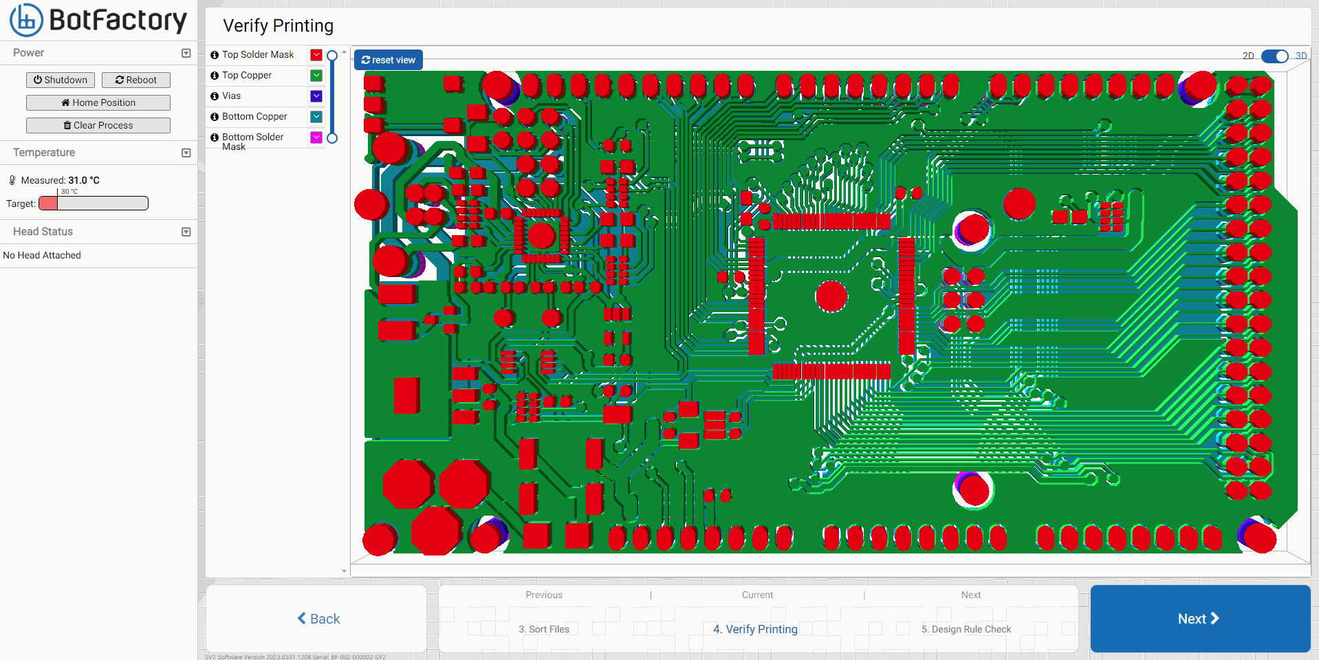
After obtaining your Gerber file, you'll need to load it into the SV2's software interface. The software will then verify your print (as shown in image below) and conduct its own Design Rule Check (DRC). It's essential to carefully review the DRC results and make any necessary adjustments to your design if significant issues are identified which ensures avoiding any bottlenecks while printing.
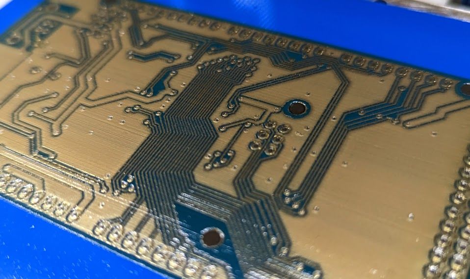
The figure on the right highlights the vias layer as printed by the SV2 printer. In the image, the dark grey conductive layers represent the uncured conductive ink. The SV2's conductive ink is engineered for optimal electrical performance and durability, ensuring a reliable and long-lasting PCB. Once the curing process is completed, these layers typically exhibit a polished, mirror-like finish. The insulating layer, responsible for the yellow tint on the PCB, is created using the SV2's insulating ink. This ink serves as a barrier between conductive layers, providing electrical insulation and preventing short circuits. Adjusting the thickness of the insulating layer can help minimize electromagnetic interference (EMI) between the top and bottom copper layers, enhancing the overall performance of the PCB.
Results
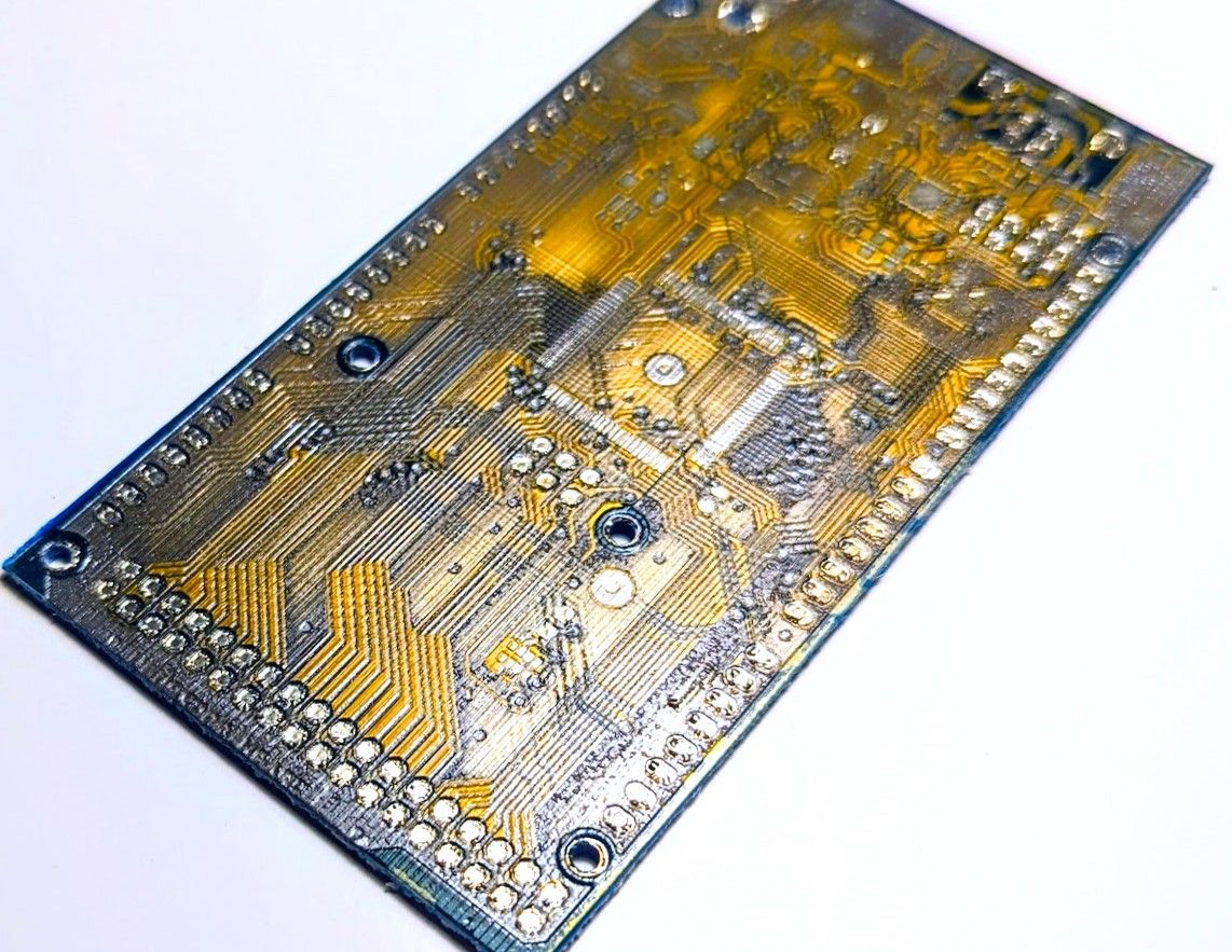
Witness the stunning final outcome of the Arduino Mega PCB, expertly printed with the exceptional BotFactory SV2 Printer, as showcased in the image on the left. Once the vias are positioned, we print the insulating mask for the top copper layer, followed by the conductive layers. Adding the finishing touch, we incorporate a final pad reinforcement using the insulating mask and conductive traces, guaranteeing outstanding soldering quality. Subsequently, holes are drilled, and rivets are inserted as required.
Our reliable PCB shears and rivet toolkits make through-hole component assembly effortless. In terms of conductivity, our 3D printed PCBs are equivalent to subtractively manufactured alternatives. As the industry progresses, the SV2 Printer continues to evolve, and our 3D printed electronic circuit boards' quality consistently improves, thanks to cutting-edge software and hardware updates. In conclusion, harness the power of the BotFactory SV2 Printer and let your Arduino Mega PCBs stand out – because who says 3D printed circuit boards can't have a touch ofswagger?
For more information, please drop some details here, we will be happy to get back to you at our earliest convenience.

