A hands-on guide to KiCad Design
For BotFactory Printers
What is a CAD tool?
A Computer Aided Design (CAD) tool is used by architects, engineers, drafters and designers to create precision drawings or technical illustrations. Instead of designing a circuit on paper and manually arranging the components, it can be done automatically with a CAD tool.
There are many different electrical CAD tools available, both free and paid. This guide will use KiCAD, an open source software that is available as a free download.

Creating a Project
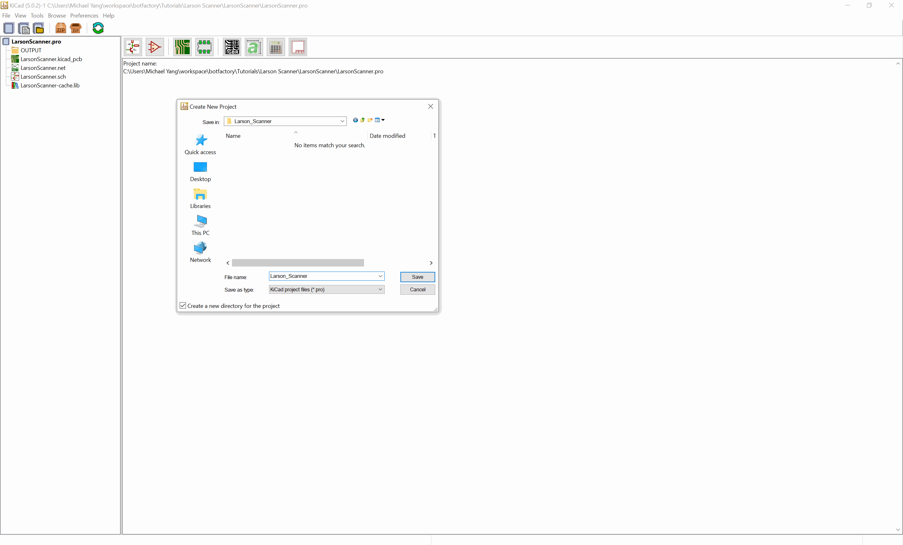
When you launch KiCAD, a existing project may or may not be pre-loaded depending on where you previously left off. We are going to ignore the existing project and create a new one.
- Navigate to File > New > Project
- Give your project a name
- Save the project in your desired directory
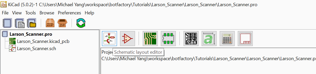
The Schematic Editor
Define the logic and architecture of your design
Schematic Editor
A schematic is a graphical representation of the logic and architecture of an electrical circuit. It shows the components and interconnections of the circuit using standardized symbolic representations. Look for the icon as shown on the right, and launch the schematic layout editor
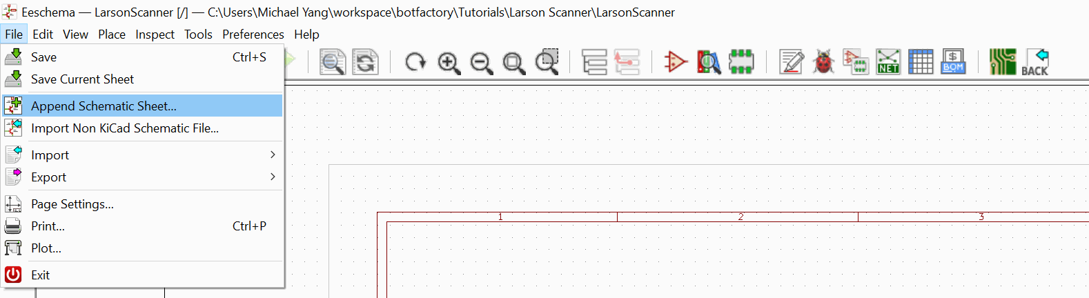
Importing your Schematic
If you already have an schematic, KiCAD supports importing existing schematics, as long as they are in a .sch format.
- Navigate to File > Append Schematic Sheet
- Select the .sch file and upload
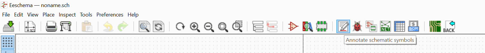
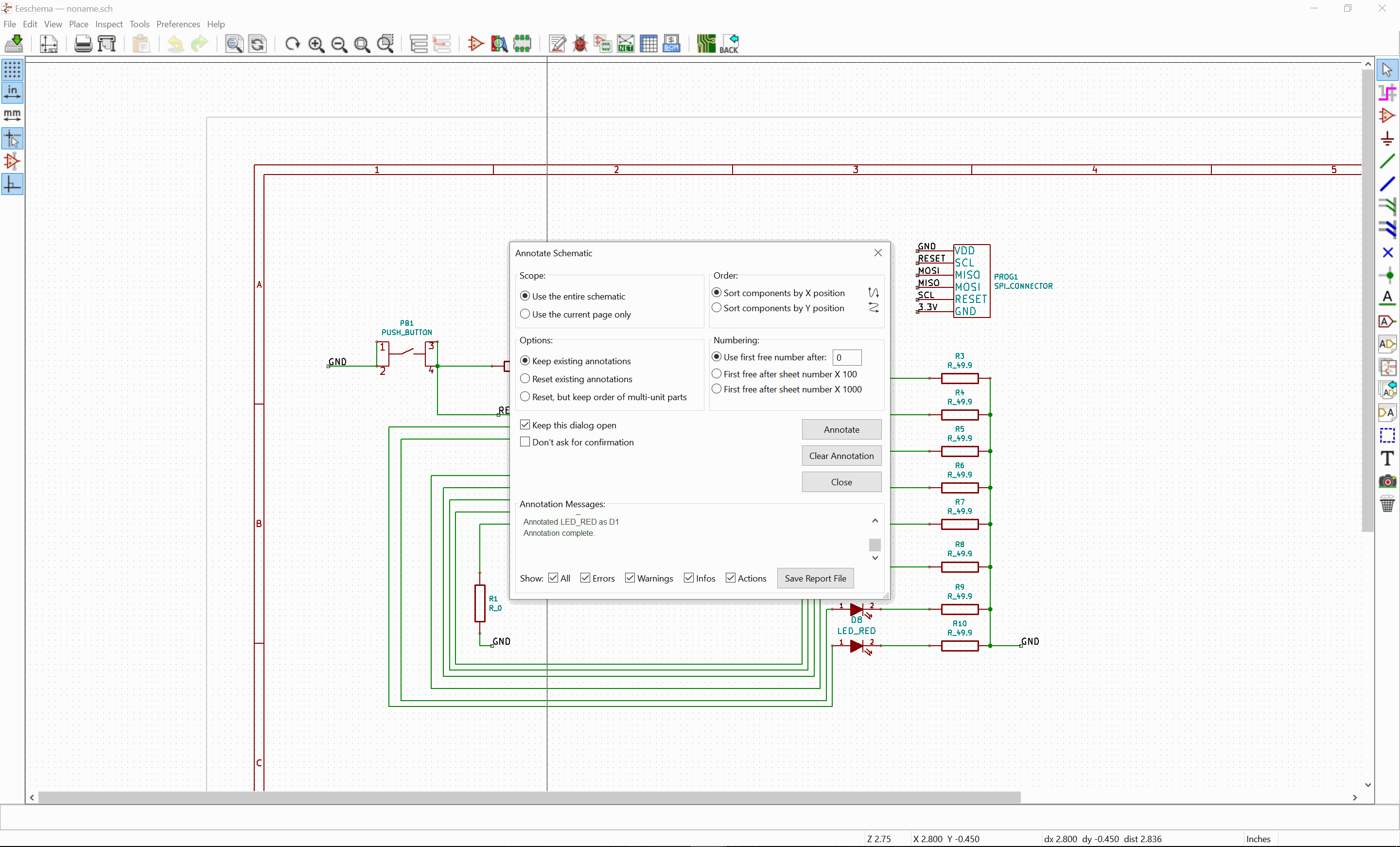
Symbol Annotation
- Look for the icon labeled "Annotate schematic symbols" as shown on the right
- Select an annotatiion order of your preference
- Click on Annotate
- Verify that all the components have a label (R0, R1, R2 etc)
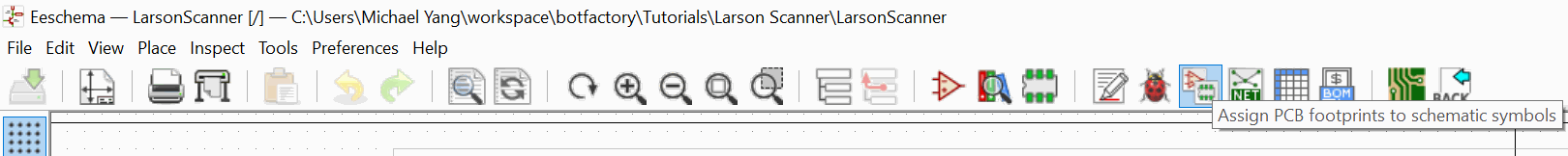
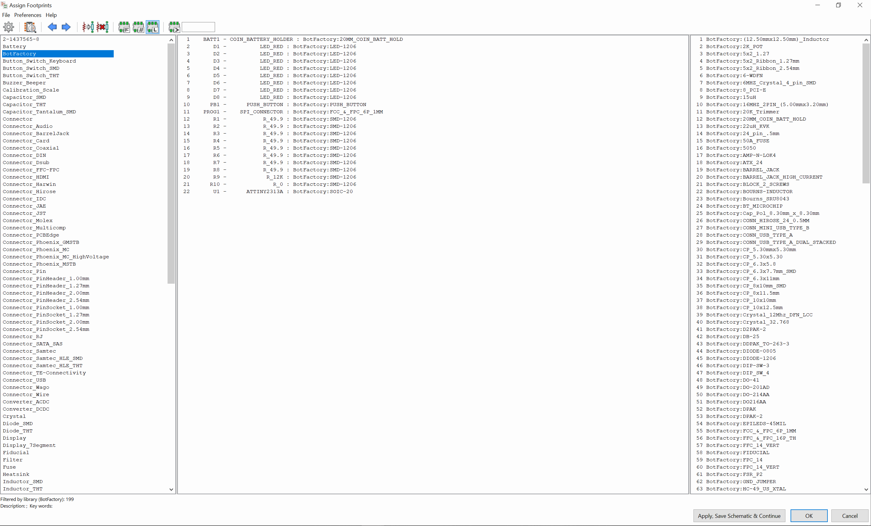
Assigning a Footprint
- Look for the icon labeled "Assign PCB footprints to schematic symbols" as shown on the right
- Assign footprints to every component
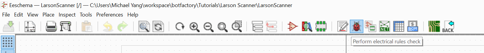
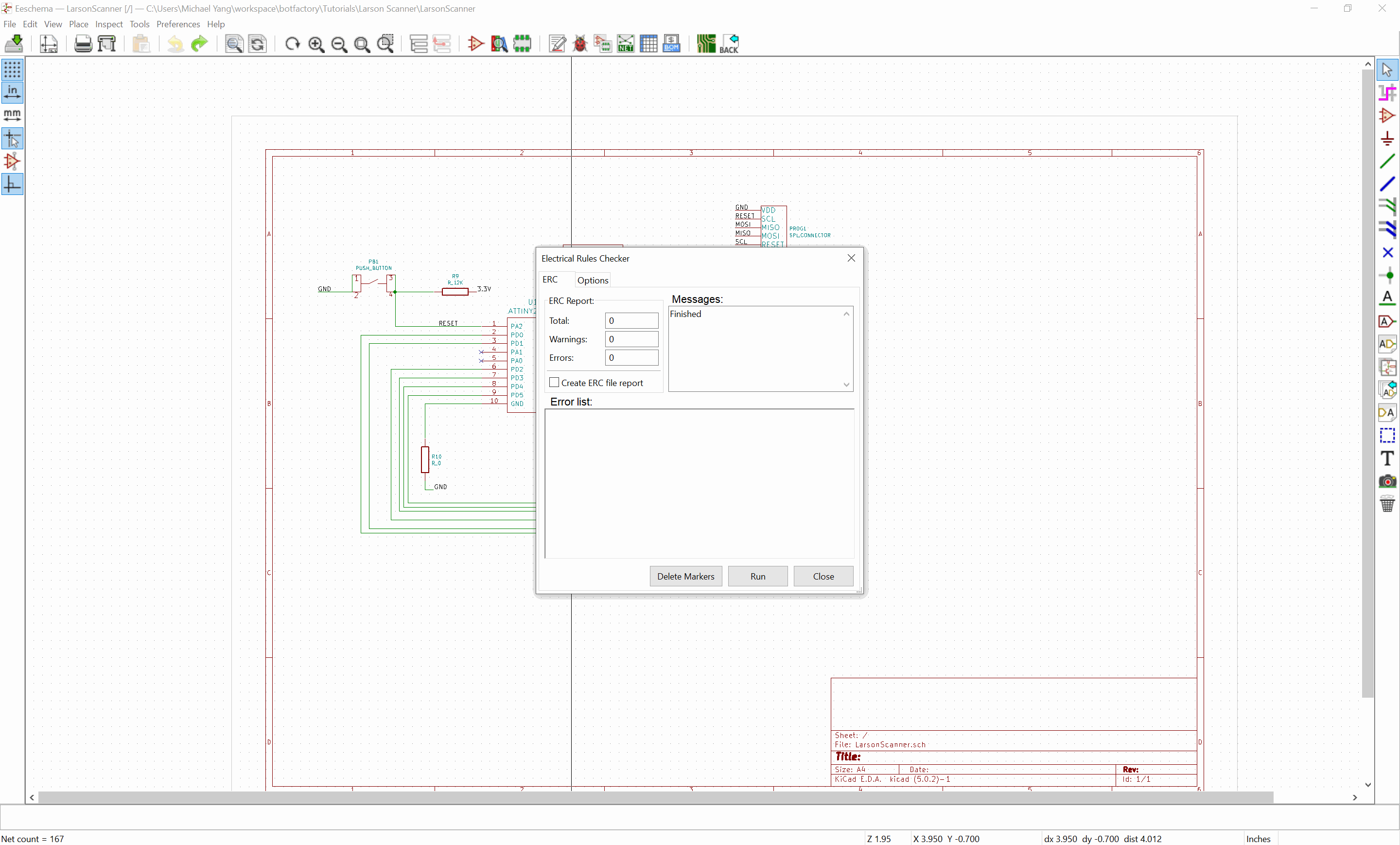
Design Rules Check
- Look for the icon labeled "Perform electrical rules check" as shown on the right
- Click on Run
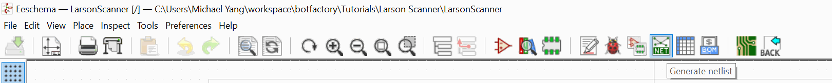
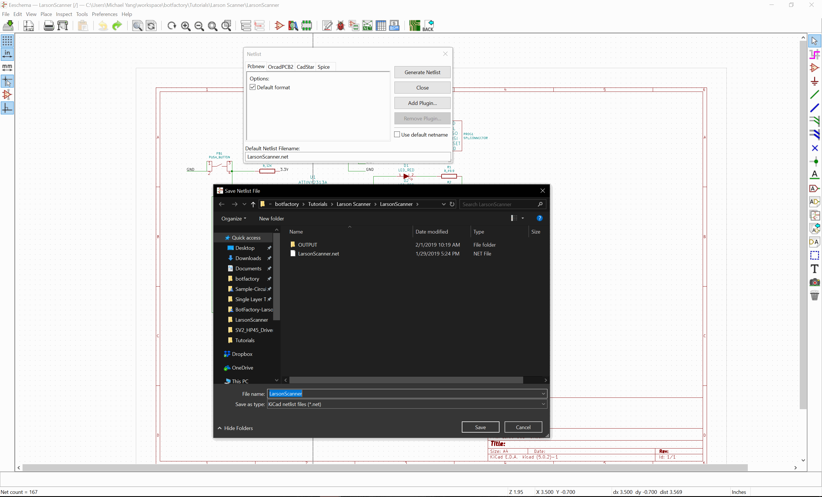
Generate a Netlist
- Look for the icon labeled "Generate netlist" as shown on the right
- Click on Generate netlist in the window that popped up
- Save the netlist in the same directory as your project
- Close the schematic editor and return to main KiCAD window
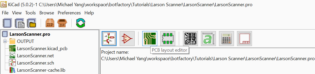
The Layout Editor
Defining the physical design of your circuit
Open the PCB Editor
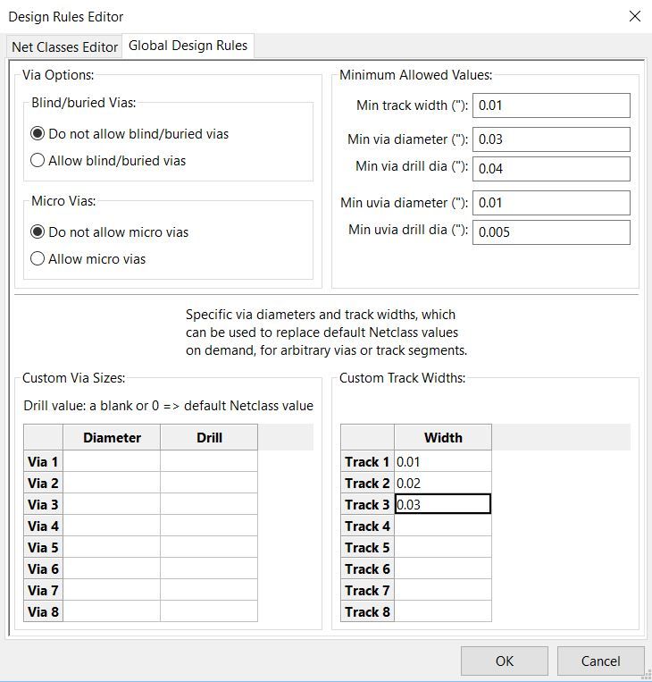
Define the Design Rules
- Click the Design Rules menu
- Select "Design Rules"
- In the "Default" net class, make sure you set the following values, according to the table below:
- Clearance
- Track Width
- Via Diameter
- Via Drill
- Then click on the "Global Design Rules", and select.
- Do not allow blind/buried vias
- Do not allow micro-vias
- Min Track Width (according to printer)
- Min Via Diameter (according to printer)
- Min Via Drill (according to printer)
- In the custom track widths tables, create the track widths that you may need in your design.
- In the custom via sizes table, create the via sizes that you may need.
| | Min Clearance | Min Track Width | Min Via Diameter | Min Via Drill |
| Squink | 12mil | 10mil | 40mil | 30mil |
| SV2 | 10mil | 8mil | 30mil | 20mil |
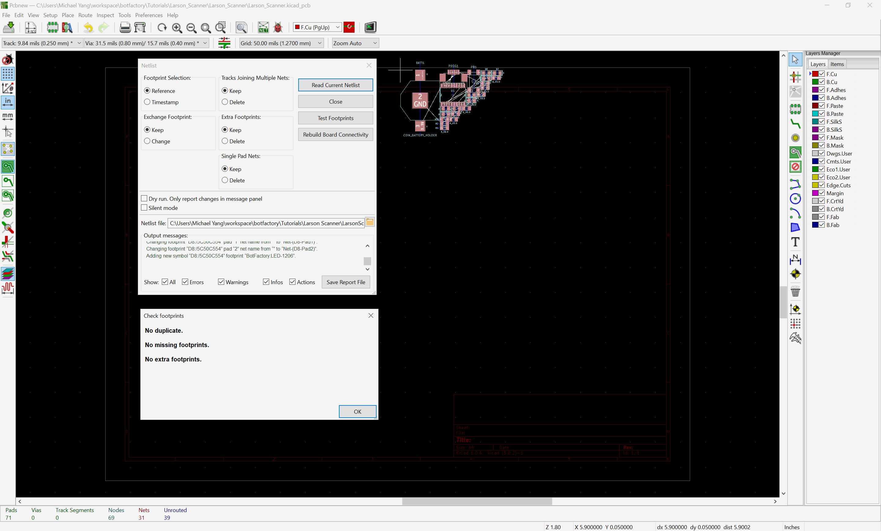
Import Netlist
- Navigate to Tools > Load Netlist
- The default directory should be the current project directory. If it is a different directory, select the current project directory
- Click on Read current netlist
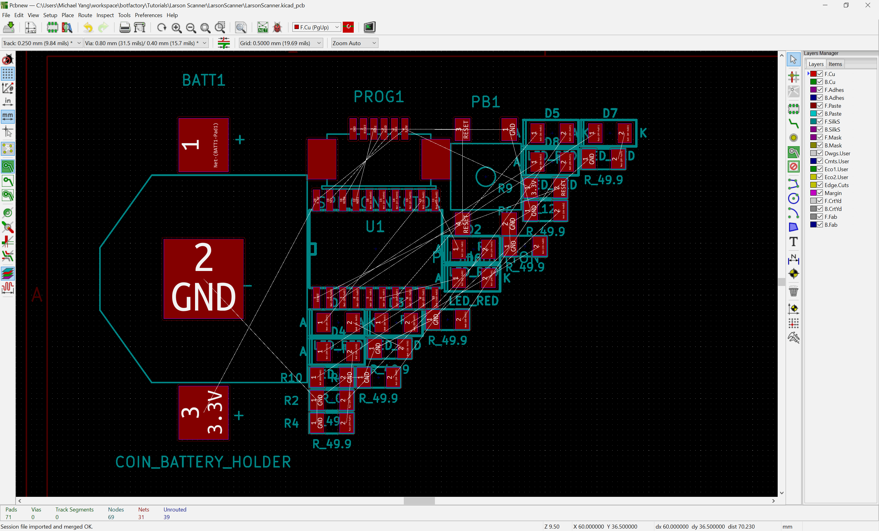
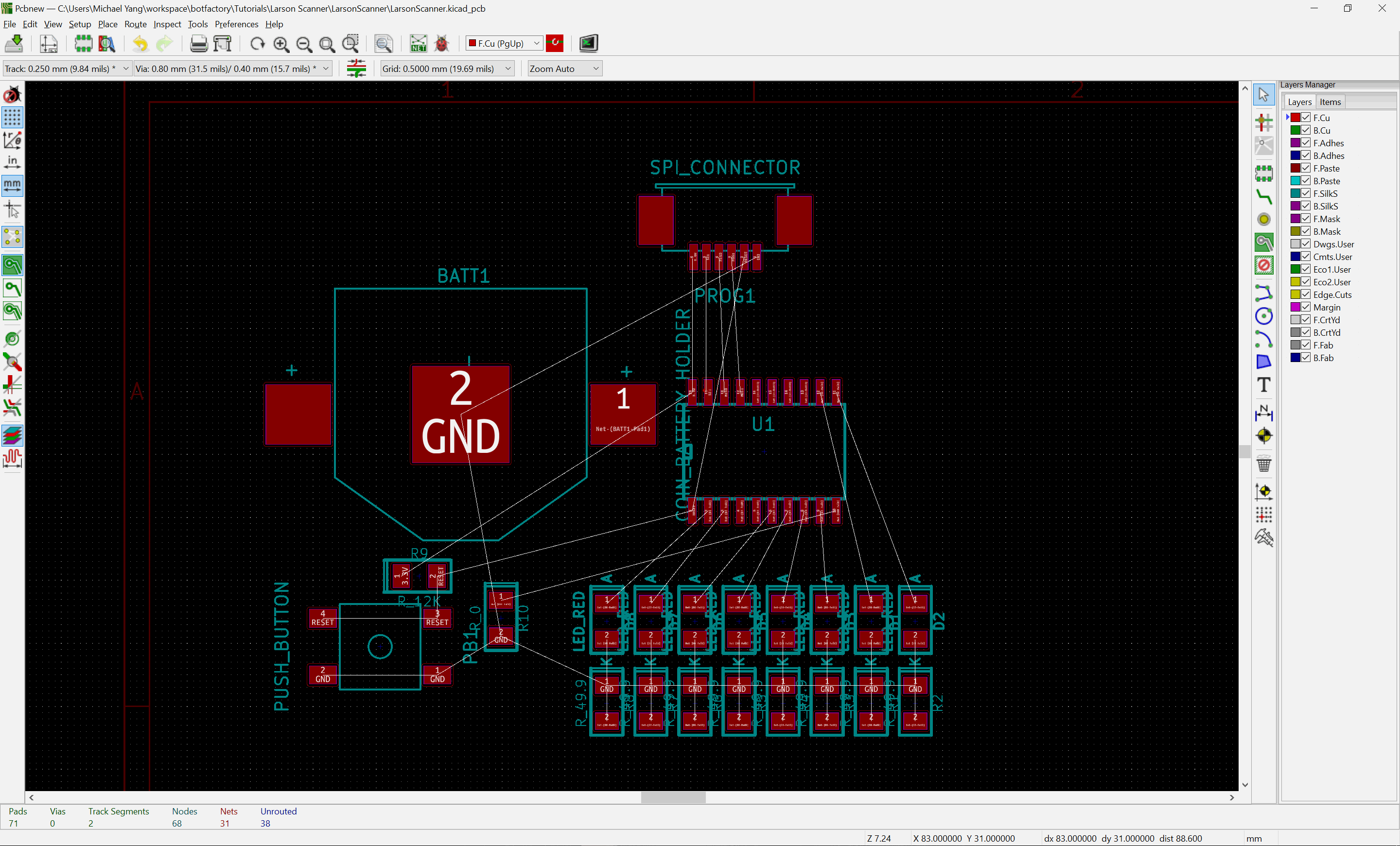
Part Layout
Arrange the parts in your desired layout.
The following is list of shortcuts that can help you in the process.
| Shortcut | Action | Description |
| M | Move | The part will now follow your cursor, use the mouse or arrow keys on the keyboard to move it around. Left click or press Enter to confirm placement |
| R | Rotate counter-clokwise | Counterclockwise The highlighted part will be rotated 90 degrees counterclockwise. |
| Shift + R | Rotate clockwise | The highlighted part will be rotated 90 degrees clockwise. |
| F | Flip | Flip the part about the surface, changing it to be back facing. |
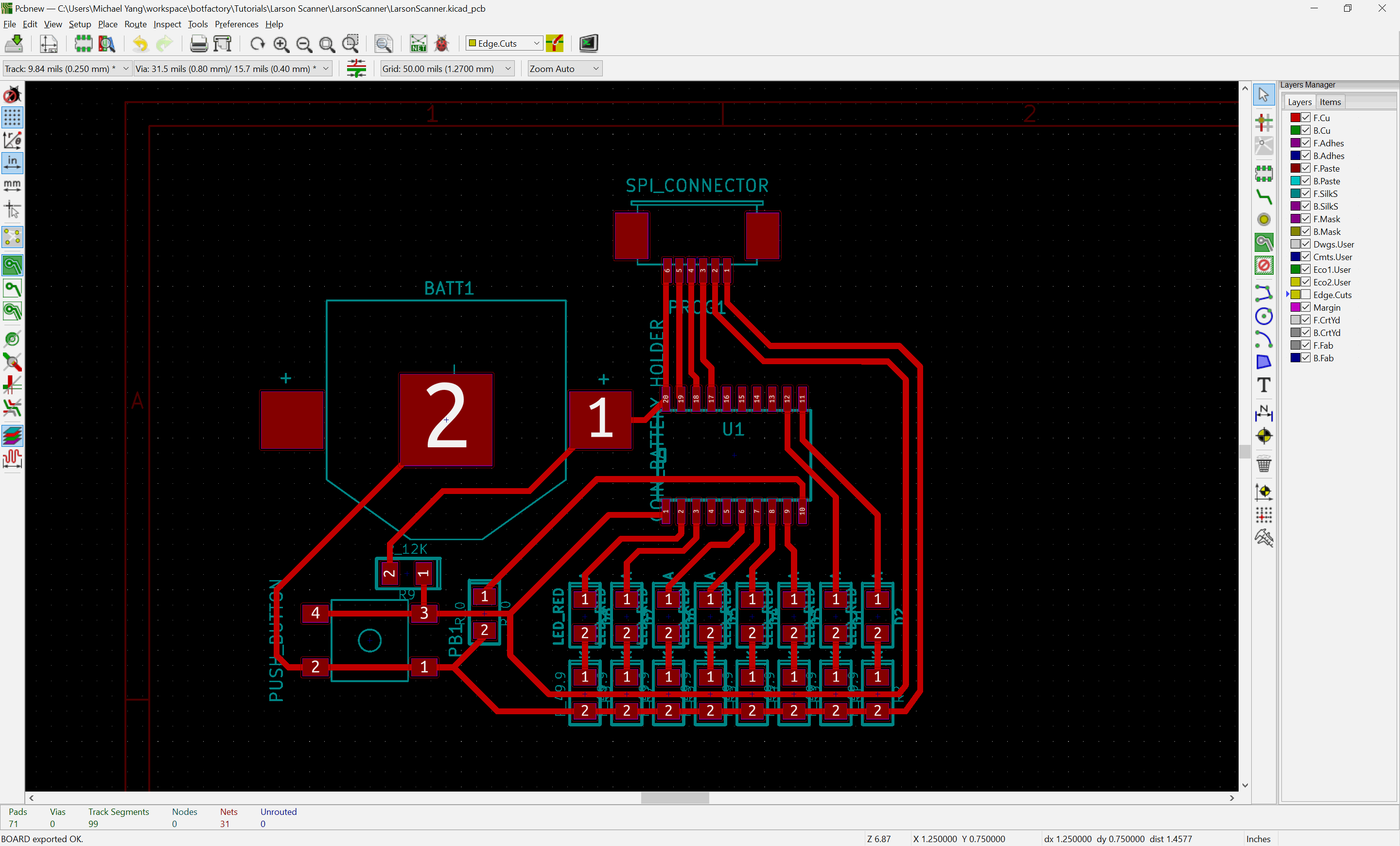
Routing
You may either route the tracks using an autorouter such as FreeRouting, or manually in KiCAD.
Note:
The track width and spacing should meet the minimum specifications of BotFactory printers.
| | Squink | SV2 |
| Trace Width | >10mil | >8mil |
| Trace spacing | >12mil | >10mil |
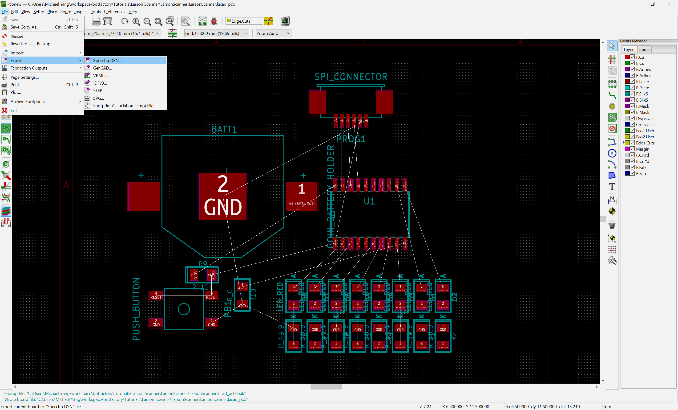
Using an autorouter:
- Navigate to File > Export > Spectra DSN
- Save the file in the project directory
- Import the DSN file into an autorouter of your choice
- Navigate to File > Import > Spectra Session and import the routed layout
Routing manually:
Route the components according to the schematic, keeping in mind the specifications provided
Tip:
Use the keyboard shortcuts below to help you:
| Shirtcut | Action | Description |
| Shift + X | Place Track | Changes cursor to track placement mode. Left click on any part to start placing a track, left clicking again on an empty space inserts an anchor point. Left click on another part joins the 2 parts together with a single track. Double click to force routing end. |
| Delete | Delete | Deletes the highlighted objet. If no object is highlighted, KiCAD will try to delete an object that the cursor is hovering above. |
| E | Properties | Opens the properties window of the highlighted track. You can adjust the track width and position. |
| G | Drag, free angle | Drags the highlighted track with the cursor. |
| D | Drag 45 degrees angle | rags the highlighted track with the cursor, maintaining a 45 degrees angle. |
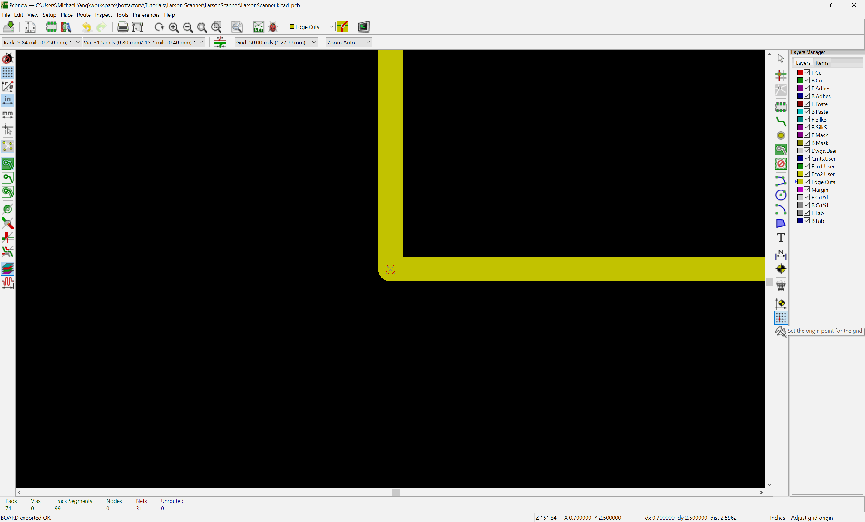
Creating an outline
An outline defines the edge of the board. It needs to be defined in order to be used with BotFactory's printers
- Make the outline layer the active layer by clicking on Edge.Cuts in the layers panel on the right.
- Click on "Add Graphical Line" next to the layers panel (keyboard shortcut: Ctrl+Shift+L"
- Enclose your circuit layout with an outline.
- Verify that your circuit layout is within the maximum dimension.
We recommend a maximum dimension of 125mm x 125mm.

Setting an origin
- Click on the button labeled "Set origin point for grid" in the right panel
- Place an auxillary axis origin at the bottom left corner of your circuit outline
- Click on the button labeled "Set origin for place and drill" in the right panel.
- Set the origin point to be the bottom left corner of your circuit outline. Aligned with the "Origin point for grid"
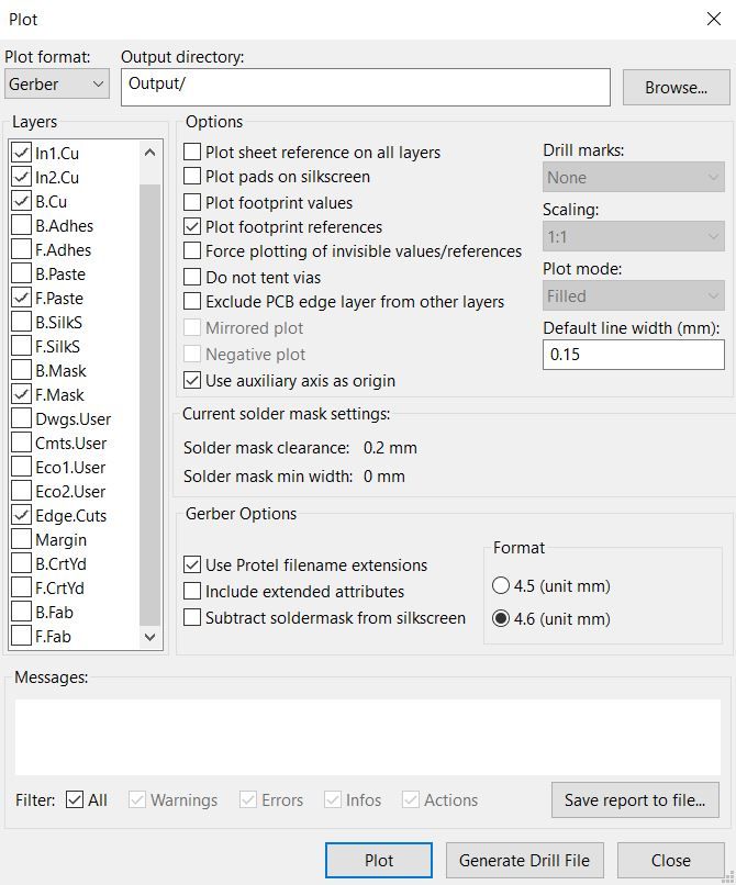
Generating the Gerber Files
Now we need to generate the gerber files that describe the PCB copper disposition in the board.
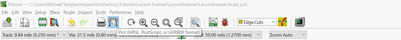
- Click on the button labeled "Plot"
- Select the layers you wish to plot. The layers required are explained in the table below.
- Select Plot Format: Gerber
- Select an output folder
- Make sure the following options are selected:
- Use auxiliary axis as origin
- Use Protel filename extensions
- Plot footprint references
- Format: 4.6mm
- Click on Plot.
The resulting files will be placed on the selected output folder. There will be one file per selected layer.
Layer Reference Guide for 2 Layers:
| Layer | Description |
| F.Cu | Front copper (top copper) |
| B.Cu | Back copper (bottom copper) |
| Edge.Cuts | Outline (edge of the board) |
| F.Mask | Top Solder mask |
| F.Paste | Top Paste layer |
| Layer | Description |
| F.Cu | Front copper (top copper) |
| In1.Cu | Internal Copper 1 (under top copper) |
| In2.Cu | Internal Copper 2 (under In1.Cu) |
| B.Cu | Back copper (bottom copper) |
| Edge.Cuts | Outline (edge of the board) |
| F.Mask | Top Solder mask |
| F.Paste | Top Paste layer |
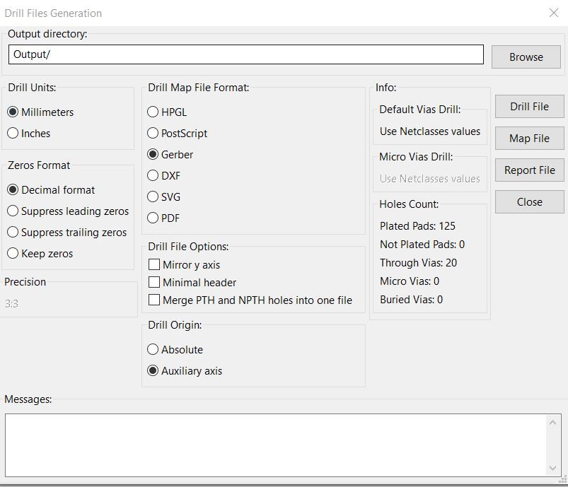
Generating the Drill Files
Now we need to generate the drill files. BotFactory printers will use drill files to create vias between the different layers.
- Click on the button labeled "Plot"
- Click on the button labeled "Generate Drill Files"
- Select an output folder
- Make sure the following options are selected:
- Drill units: Millimiters
- Zeros Format: Decimal
- Drill Origin: Auxiliary Axis
- Click on "Drill File"
The resulting file will be placed on the selected output folder. There will be one drill file for the whole circuit if micro-vias or buried vias
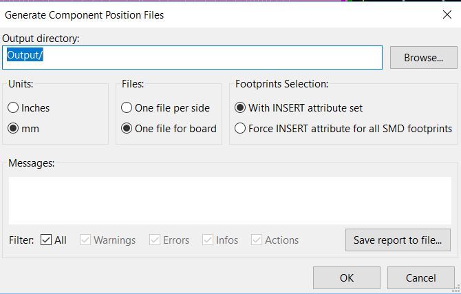
Generating the PnP files (center and rotation)
Now we need to generate the center and rotation files for the Pick and Place process.
- Click on the file menu
- Select "Fabrication outputs"
- Select "Footprint position"
- Select the output folder
- Make sure the following options are selected:
- Units: Millimiters
- Fooprint selection: With Insert attribute
- Click "OK"
The resulting file will be placed on the selected output folder.
Final Check
Navigate to the output folder you previously selected, and verify that you have these files in the folder.
<Project Name>-Edge.Cuts.gbr
<Project Name>-F.Cu.gbr
<Project Name>-F.Paste.gbr
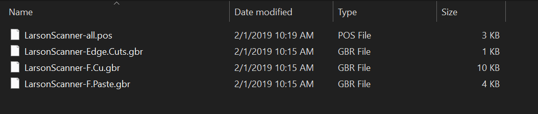
Uploading files to printer
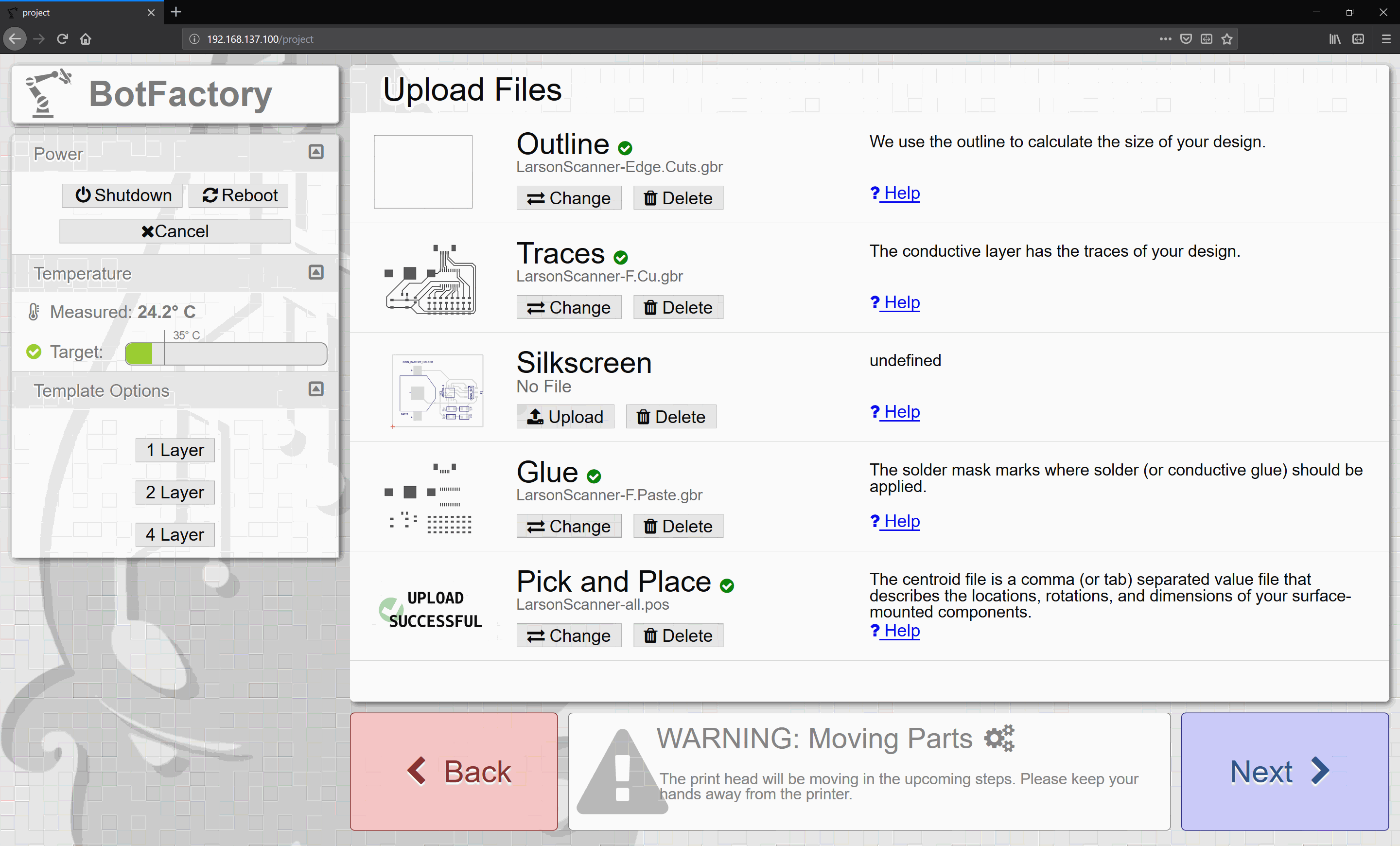
| Layer | File |
| Outline | Edge.Cuts.gbr |
| Traces | F.Cu.gbr |
| Glue | F.Paste.gbr |
| Pick and Place | all.pos |